Introduction
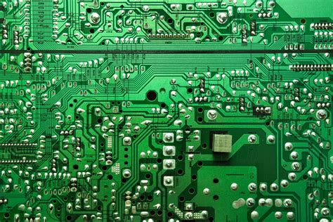
In today’s world of high-speed electronics and densely packed printed circuit boards (PCBs), electromagnetic interference (EMI) has become a significant concern for designers and engineers. EMI can cause undesirable effects on the performance and reliability of electronic devices, leading to malfunctions, data corruption, and even complete system failures. To mitigate these issues, it is crucial to implement effective EMI-reducing PCB shielding techniques in your designs. In this article, we will explore various methods and strategies to shield your PCBs from EMI, ensuring optimal performance and compliance with electromagnetic compatibility (EMC) regulations.
Understanding EMI and Its Sources
Before diving into the shielding techniques, it is essential to understand what EMI is and how it originates. EMI refers to the unwanted electromagnetic energy that interferes with the normal operation of electronic devices. It can be generated by various sources, both internal and external to the device. Some common sources of EMI include:
- High-speed digital circuits
- Switching power supplies
- Wireless communication modules
- Electrostatic discharge (ESD)
- External electromagnetic fields from nearby devices or power lines
EMI can propagate through different mechanisms, such as conduction, radiation, and coupling. Conducted EMI travels along the power lines, signal traces, and ground planes of the PCB, while radiated EMI propagates through the air as electromagnetic waves. Coupling occurs when the electromagnetic fields from one component or trace induce unwanted signals in nearby components or traces.
PCB Shielding Materials and Techniques
To effectively shield your PCBs from EMI, you can employ various materials and techniques. Let’s explore some of the most common and effective options:
1. Grounding and Shielding Planes
One of the fundamental techniques for EMI reduction is the proper use of grounding and shielding planes on the PCB. A solid ground plane provides a low-impedance return path for high-frequency currents, minimizing the loop area and reducing EMI radiation. Shielding planes, typically made of copper, act as barriers to block the propagation of electromagnetic waves.
When designing your PCB, consider the following guidelines for effective grounding and shielding:
- Use a continuous and uninterrupted ground plane on one or more layers of the PCB.
- Minimize the distance between the ground plane and the signal traces to reduce loop area.
- Use ground stitching vias to connect the ground planes on different layers, providing a low-impedance path for high-frequency currents.
- Implement shielding planes on the top and bottom layers of the PCB to create a Faraday cage-like structure.
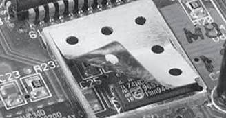
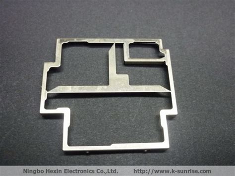
2. EMI Shielding Enclosures
EMI shielding enclosures are metallic containers that surround the sensitive components or entire PCBs to protect them from external EMI sources. These enclosures act as a barrier, reflecting or absorbing the electromagnetic waves and preventing them from entering or escaping the shielded area.
When selecting an EMI shielding enclosure, consider the following factors:
- Material: Choose a material with high electrical conductivity and magnetic permeability, such as aluminum, copper, or nickel-plated steel.
- Thickness: Ensure the enclosure walls are thick enough to provide adequate shielding effectiveness across the desired frequency range.
- Seams and openings: Minimize the number and size of seams and openings in the enclosure, as they can compromise the shielding performance. Use conductive gaskets or EMI-shielding tapes to seal any necessary openings.
- Grounding: Properly ground the enclosure to the PCB’s ground plane to ensure a low-impedance path for high-frequency currents.
3. EMI Shielding Components
In addition to enclosures, there are various EMI shielding components that can be incorporated into your PCB design to mitigate specific EMI issues. These components include:
- Ferrite beads: Ferrite beads are passive components that act as high-frequency filters, suppressing high-frequency noise on power lines and signal traces. They are particularly effective in reducing conducted EMI.
- Common-mode chokes: Common-mode chokes are transformers designed to attenuate common-mode noise, which is the noise that appears simultaneously on both the signal and return paths. They are commonly used on differential signal lines, such as USB or Ethernet.
- EMI filters: EMI filters are passive or active circuits that selectively attenuate unwanted high-frequency signals while allowing the desired signals to pass through. They typically consist of capacitors, inductors, and resistors in various configurations.
- Shielded connectors: Shielded connectors, such as shielded USB or Ethernet connectors, provide an additional layer of EMI protection at the interface between the PCB and external cables.
4. PCB Layout Techniques
Proper PCB layout techniques play a crucial role in reducing EMI and ensuring the overall EMC of your design. Here are some key layout guidelines to follow:
- Minimize loop areas: Keep the loop areas formed by signal traces and their return paths as small as possible to reduce magnetic field coupling and radiated EMI.
- Separate sensitive signals: Physically separate sensitive analog and digital signals to minimize crosstalk and interference.
- Use guard traces: Implement guard traces, which are grounded traces running parallel to sensitive signal traces, to provide additional shielding and reduce crosstalk.
- Avoid split ground planes: Avoid splitting the ground plane, as it can create high-impedance paths for return currents and increase EMI. If splitting is necessary, use stitching capacitors to maintain a low-impedance connection between the split sections.
- Route traces on inner layers: Whenever possible, route sensitive signal traces on the inner layers of the PCB, as they are naturally shielded by the power and ground planes on the outer layers.

Testing and Validation
Once you have implemented the EMI-reducing PCB shielding techniques in your design, it is essential to test and validate the effectiveness of the shielding. EMC testing can be performed in specialized labs equipped with anechoic chambers and EMI measurement equipment. The following tests are commonly conducted to assess the EMC performance of a PCB:
- Radiated emissions test: This test measures the electromagnetic fields emitted by the PCB and ensures they are within the limits specified by relevant EMC standards, such as FCC Part 15 or CISPR 22.
- Conducted emissions test: This test measures the EMI conducted through the power lines and cables connected to the PCB, ensuring compliance with conducted emission limits.
- Radiated immunity test: This test evaluates the PCB’s ability to function correctly in the presence of external electromagnetic fields, simulating real-world EMI scenarios.
- Conducted immunity test: This test assesses the PCB’s resilience to conducted EMI, such as electrical fast transients (EFTs) and surge pulses, which can propagate through the power lines or signal cables.
By conducting thorough EMC testing, you can identify any remaining EMI issues and make necessary adjustments to your design to achieve optimal shielding performance.
Frequently Asked Questions (FAQ)
1. What is the difference between EMI and EMC?
EMI (Electromagnetic Interference) refers to the unwanted electromagnetic energy that interferes with the normal operation of electronic devices. EMC (Electromagnetic Compatibility) is the ability of an electronic device to function properly in its electromagnetic environment without causing or being susceptible to EMI.
2. Can EMI cause permanent damage to electronic devices?
In most cases, EMI does not cause permanent damage to electronic devices. However, severe EMI events, such as strong electromagnetic pulses (EMPs) or sustained exposure to high-intensity fields, can potentially damage sensitive components or cause long-term reliability issues.
3. How do I choose the right EMI shielding material for my PCB?
The choice of EMI shielding material depends on factors such as the frequency range of concern, the required shielding effectiveness, the operating environment, and the cost. Common shielding materials include aluminum, copper, nickel-plated steel, and conductive plastics. Consult with EMI shielding experts or refer to EMC guidelines to select the most suitable material for your specific application.
4. Can software techniques be used to reduce EMI?
While hardware shielding techniques are the primary means of reducing EMI, software techniques can also play a role in minimizing EMI generation. For example, using spread-spectrum clocking, implementing noise-canceling algorithms, and optimizing code to reduce high-frequency transitions can help reduce the overall EMI signature of a device.
5. How often should I perform EMC testing on my PCB design?
EMC testing should be performed at various stages of the product development cycle, including initial prototyping, pre-compliance testing, and final compliance testing. It is recommended to conduct EMC testing whenever significant changes are made to the PCB design, components, or firmware to ensure ongoing compliance with EMC regulations.
Conclusion
Incorporating EMI-reducing PCB shielding techniques in your designs is crucial for ensuring the reliable operation of electronic devices and compliance with EMC regulations. By understanding the sources and propagation mechanisms of EMI, selecting appropriate shielding materials and components, following best practices for PCB layout, and conducting thorough EMC testing, you can effectively mitigate EMI issues and achieve optimal performance in your designs.
Remember, EMI shielding is not a one-size-fits-all solution, and the specific techniques and materials used may vary depending on the application, frequency range, and environmental factors. Continuously staying updated with the latest advancements in EMI shielding technologies and collaborating with EMC experts can help you stay ahead of the curve in designing robust and EMI-resistant PCBs.
| EMI Shielding Technique | Description |
|---|---|
| Grounding and Shielding Planes | Use continuous ground planes and shielding planes on PCB layers to provide low-impedance return paths and block EMI propagation. |
| EMI Shielding Enclosures | Surround sensitive components or entire PCBs with metallic enclosures to reflect or absorb electromagnetic waves. |
| EMI Shielding Components | Incorporate components such as ferrite beads, common-mode chokes, EMI filters, and shielded connectors to suppress specific EMI issues. |
| PCB Layout Techniques | Minimize loop areas, separate sensitive signals, use guard traces, avoid split ground planes, and route traces on inner layers to reduce EMI. |
By implementing these EMI-reducing PCB shielding techniques and following the guidelines discussed in this article, you can create designs that are more resilient to EMI, ensuring the reliability and performance of your electronic devices in today’s increasingly complex electromagnetic environment.
No responses yet