Introduction to Embedded PCBs
Embedded PCBs, also known as multi-layer circuit boards with embedded components, are revolutionizing the electronics industry by offering a more compact, efficient, and reliable solution for modern electronic devices. Unlike traditional printed circuit boards (PCBs), embedded PCBs incorporate components within the layers of the board itself, creating a highly integrated and space-saving design.
What is an Embedded PCB?
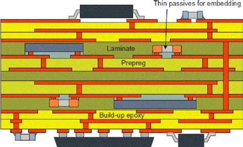
An embedded PCB is a multi-layer circuit board that contains components embedded within its layers. These components can include passive elements such as resistors, capacitors, and inductors, as well as active components like integrated circuits (ICs) and semiconductors. By embedding these components within the board, designers can achieve a more compact and efficient layout, reducing the overall size and weight of the electronic device.
Advantages of Embedded PCBs
Embedded PCBs offer several advantages over traditional PCBs:
-
Space Savings: By embedding components within the board, designers can significantly reduce the surface area required for the circuit, leading to smaller and more compact devices.
-
Improved Performance: Embedded components are placed closer to the other components they interact with, reducing the length of interconnects and minimizing signal loss and interference.
-
Enhanced Reliability: With fewer external connections and a more robust construction, embedded PCBs are less susceptible to mechanical stress and environmental factors, resulting in improved reliability.
-
Reduced Assembly Time: Embedding components eliminates the need for manual placement and soldering, streamlining the assembly process and reducing production time.
Manufacturing Process of Embedded PCBs
Step 1: Substrate Preparation
The manufacturing process of an embedded PCB begins with the preparation of the substrate material, typically a glass-reinforced epoxy laminate (e.g., FR-4). The substrate is cleaned and treated to ensure proper adhesion of the subsequent layers.
Step 2: Cavity Creation
Using precise machining techniques, such as laser drilling or mechanical milling, cavities are created within the substrate to accommodate the embedded components. The size and shape of the cavities depend on the specific components being embedded.
Step 3: Component Placement
The embedded components are carefully placed into the cavities created in the substrate. This process can be done manually or using automated pick-and-place machines for higher precision and efficiency.
Step 4: Lamination
Once the components are in place, additional layers of substrate material are laminated on top of the base layer, encapsulating the embedded components. The lamination process involves applying heat and pressure to bond the layers together, creating a solid and cohesive structure.
Step 5: Via Formation
After lamination, vias are formed to create electrical connections between the embedded components and the surface layers of the PCB. Vias can be drilled mechanically or using laser technology, depending on the required size and precision.
Step 6: Circuit Patterning
The outer layers of the PCB are then patterned with the desired circuit design using a combination of photolithography and etching processes. This step creates the conductive traces that interconnect the embedded components with other surface-mounted components and connectors.
Step 7: Surface Finishing
Finally, the PCB undergoes a surface finishing process to protect the exposed copper traces and improve solderability. Common surface finishes include hot air solder leveling (HASL), immersion silver, immersion tin, and electroless nickel immersion gold (ENIG).

Design Considerations for Embedded PCBs
When designing an embedded PCB, several key factors must be considered to ensure optimal performance and manufacturability:
Component Selection
Choosing the right components for embedding is crucial. Designers must consider factors such as size, thermal characteristics, and compatibility with the embedding process. Some components, such as certain ceramic capacitors and resistors, are well-suited for embedding due to their small size and robustness.
Thermal Management
Embedded components generate heat during operation, which can affect the performance and reliability of the PCB. Proper thermal management techniques, such as using thermal vias or embedding heat spreaders, must be employed to dissipate heat effectively and maintain optimal operating temperatures.
Signal Integrity
Embedding components can impact the signal integrity of the PCB, particularly at high frequencies. Designers must carefully analyze and simulate the signal paths to ensure proper impedance matching, minimize crosstalk, and reduce electromagnetic interference (EMI).
Manufacturing Constraints
The manufacturing process for embedded PCBs imposes certain constraints on the design. For example, the size and position of the embedded components must be carefully considered to ensure they fit within the available space and do not interfere with the drilling of vias or the patterning of circuits. Designers must work closely with the manufacturing team to ensure the design is feasible and cost-effective to produce.

Applications of Embedded PCBs
Embedded PCBs find applications in a wide range of industries and products where miniaturization, performance, and reliability are critical:
Consumer Electronics
Smartphones, smartwatches, and other wearable devices benefit greatly from embedded PCBs. The compact and efficient design allows for smaller form factors and longer battery life, while the improved performance and reliability enhance the user experience.
Automotive Electronics
In the automotive industry, embedded PCBs are used in various electronic control units (ECUs), sensors, and infotainment systems. The rugged construction and enhanced reliability of embedded PCBs make them well-suited for the harsh operating conditions found in vehicles.
Medical Devices
Medical devices, such as implantable sensors and wearable health monitors, require highly miniaturized and reliable electronics. Embedded PCBs enable the development of compact and robust medical devices that can withstand the rigors of long-term use in the human body.
Aerospace and Defense
Embedded PCBs are essential for aerospace and defense applications, where space is at a premium and reliability is paramount. From satellite systems to avionics and military communications equipment, embedded PCBs provide the necessary performance and durability in these demanding environments.

Future Trends and Developments
As technology continues to advance, the demand for smaller, faster, and more efficient electronic devices will only increase. Embedded PCBs will play a crucial role in meeting these demands, and several trends and developments are expected to shape the future of this technology:
Advanced Materials
Researchers are exploring new substrate materials and embedding compounds that offer better thermal, mechanical, and electrical properties. These advanced materials will enable the development of even more compact and high-performance embedded PCBs.
3D Embedding Techniques
While current embedded PCBs primarily focus on embedding components within a single plane, future developments may involve true three-dimensional (3D) embedding techniques. This approach would allow for even greater space savings and design flexibility by stacking components vertically within the board.
Integration of Optical Components
As data transmission rates continue to increase, the integration of optical components, such as waveguides and optical fibers, into embedded PCBs may become more prevalent. This integration would enable high-speed, low-loss data transmission within the board, further enhancing the performance of electronic devices.
Artificial Intelligence and Machine Learning
The application of artificial intelligence (AI) and machine learning techniques in the design and manufacturing of embedded PCBs could lead to more optimized and efficient designs. AI-driven design tools could automatically generate layouts that maximize performance and minimize manufacturing costs, while machine learning algorithms could optimize the embedding process for improved yield and reliability.
FAQs
Q1: Can all components be embedded in a PCB?
A1: Not all components are suitable for embedding. Components that are too large or generate excessive heat may not be good candidates for embedding. Additionally, some components, such as connectors and user interface elements, need to be accessible from the surface of the board.
Q2: How does the cost of an embedded PCB compare to a traditional PCB?
A2: The cost of an embedded PCB is generally higher than that of a traditional PCB due to the more complex manufacturing process and specialized materials required. However, the overall cost of the end product may be lower due to the reduced size and improved performance of the embedded PCB.
Q3: Are embedded PCBs more difficult to repair than traditional PCBs?
A3: Yes, embedded PCBs can be more challenging to repair since the embedded components are not accessible from the surface. In some cases, a faulty embedded component may require the complete replacement of the PCB.
Q4: How do embedded PCBs handle electromagnetic interference (EMI)?
A4: Embedded PCBs can provide better EMI shielding compared to traditional PCBs due to the closer proximity of the components and the use of ground planes within the board. However, careful design and layout are still necessary to minimize EMI and ensure compliance with relevant standards.
Q5: Can embedded PCBs be used in high-temperature environments?
A5: Yes, embedded PCBs can be designed to operate in high-temperature environments by selecting appropriate materials and components. However, proper thermal management techniques must be employed to ensure the embedded components do not overheat and degrade the performance of the board.
Conclusion
Embedded PCBs represent a significant advancement in electronic packaging and circuit board design. By integrating components within the layers of the board, embedded PCBs offer numerous benefits, including space savings, improved performance, enhanced reliability, and reduced assembly time. As technology continues to progress, embedded PCBs will play an increasingly important role in enabling the development of smaller, faster, and more efficient electronic devices across a wide range of industries.
However, designing and manufacturing embedded PCBs comes with its own set of challenges and considerations. Designers must carefully select components, manage thermal dissipation, ensure signal integrity, and work within manufacturing constraints to create successful embedded PCB designs. As new materials, techniques, and technologies emerge, the capabilities of embedded PCBs will continue to expand, pushing the boundaries of what is possible in electronic packaging and circuit board design.
As the demand for more compact, high-performance electronic devices continues to grow, embedded PCBs will undoubtedly remain at the forefront of innovation in the electronics industry. By understanding the principles, advantages, and challenges associated with embedded PCBs, designers and manufacturers can leverage this technology to create the next generation of cutting-edge electronic products that shape our world.
No responses yet