Introduction to EMI and its Impact on Electronic Systems
Electromagnetic interference (EMI) is a major concern in the design and development of electronic systems. EMI can cause unwanted disturbances, malfunctions, and even failures in electronic devices, leading to reduced performance, reliability issues, and non-compliance with regulatory standards. As electronic systems become more complex and operate at higher frequencies, the risk of EMI-related problems increases significantly.
To mitigate EMI issues and ensure the proper functioning of electronic devices, it is crucial to address EMI concerns at the design stage itself. By implementing robust EMI design rule checks (EMI-DRC) and conducting plane resonance analysis, designers can identify and resolve potential EMI problems early in the development process, saving time, effort, and costs associated with later-stage fixes and redesigns.
Understanding EMI Design Rule Check (EMI-DRC)
EMI Design Rule Check (EMI-DRC) is a proactive approach to identifying and addressing potential EMI issues during the design phase of electronic systems. It involves a set of guidelines, rules, and best practices that designers can follow to minimize the risk of EMI-related problems. EMI-DRC covers various aspects of electronic design, including:
- PCB layout and routing
- Component placement and orientation
- Power distribution network design
- Signal integrity and crosstalk management
- Shielding and grounding techniques
By adhering to EMI-DRC guidelines, designers can create more robust and EMI-resistant electronic systems, reducing the likelihood of EMI-related failures and ensuring compliance with relevant EMC (Electromagnetic Compatibility) standards.
Key Elements of EMI-DRC
To effectively implement EMI-DRC in the design process, designers should focus on the following key elements:
1. PCB Layout and Routing
Proper PCB layout and routing are essential for minimizing EMI. Some important considerations include:
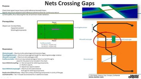
- Minimizing loop areas to reduce magnetic field coupling
- Avoiding long, parallel traces to reduce crosstalk
- Using ground planes to provide a low-impedance return path for high-frequency currents
- Separating sensitive signals from noisy signals to minimize interference
2. Component Placement and Orientation
The placement and orientation of components on a PCB can significantly impact EMI performance. Designers should:
- Place sensitive components away from noisy components
- Orient components to minimize coupling between them
- Use shielding techniques, such as metal cans or shielding gaskets, to isolate sensitive components
3. Power Distribution Network Design
A well-designed power distribution network (PDN) is crucial for minimizing EMI. Key considerations include:
- Using decoupling capacitors to reduce power supply noise
- Placing decoupling capacitors close to the power pins of ICs
- Using power planes to provide a low-impedance power distribution
- Implementing proper power sequencing to avoid sudden current spikes
4. Signal Integrity and Crosstalk Management
Maintaining signal integrity and minimizing crosstalk are essential for reducing EMI. Designers should:
- Use appropriate termination techniques to minimize reflections and ringing
- Implement differential signaling for high-speed interfaces
- Use guard traces or ground shields to isolate sensitive signals
- Control rise and fall times of digital signals to minimize high-frequency content
5. Shielding and Grounding Techniques
Effective shielding and grounding are critical for EMI mitigation. Some important techniques include:
- Using conductive enclosures to shield sensitive circuits
- Implementing proper grounding strategies, such as star grounding or multi-point grounding
- Using shielded cables and connectors for external connections
- Providing adequate bonding and grounding of shields to the chassis or enclosure
By focusing on these key elements of EMI-DRC, designers can create more robust and EMI-resistant electronic systems, reducing the risk of EMI-related problems and ensuring compliance with relevant EMC standards.

Plane Resonance Analysis: A Crucial Tool for EMI Mitigation
Plane resonance is a phenomenon that occurs in power and ground planes of multilayer PCBs, where the planes act as cavity resonators at certain frequencies. These resonances can lead to significant EMI issues, such as increased radiated emissions and degraded signal integrity. To effectively mitigate EMI problems, it is essential to perform plane resonance analysis during the design stage.
Understanding Plane Resonance
Plane resonance occurs when the dimensions of the power and ground planes on a PCB are comparable to the wavelength of the signals propagating through them. At these resonant frequencies, the planes can support standing waves, leading to voltage fluctuations and increased EMI.
The resonant frequencies of a rectangular plane can be calculated using the following equation:
f(m,n) = c / (2 * sqrt(εr)) * sqrt((m/a)^2 + (n/b)^2)
Where:
– f(m,n) is the resonant frequency for the (m,n) mode
– c is the speed of light in vacuum
– εr is the relative permittivity of the dielectric material
– a and b are the length and width of the plane, respectively
– m and n are integers representing the mode numbers
By understanding the factors that influence plane resonance, designers can take appropriate measures to mitigate its effects on EMI.
Techniques for Mitigating Plane Resonance
Several techniques can be employed to mitigate the impact of plane resonance on EMI:
1. Proper Plane Sizing
Designers should carefully choose the dimensions of power and ground planes to avoid resonances at critical frequencies. By adjusting the plane sizes, resonant frequencies can be shifted away from the frequency range of interest.
2. Plane Segmentation
Dividing large power and ground planes into smaller segments can help disrupt the formation of standing waves and reduce the impact of plane resonance. This can be achieved by using split planes or by introducing slots or cutouts in the planes.
3. Decoupling Capacitor Placement
Strategically placing decoupling capacitors can help suppress plane resonances by providing a low-impedance path for high-frequency currents. Capacitors should be placed close to the power pins of ICs and distributed evenly across the PCB.
4. Use of Embedded Capacitance Materials
Embedded capacitance materials, such as high-k dielectrics, can be used in the PCB stackup to provide distributed capacitance between the power and ground planes. This helps to suppress plane resonances and reduce EMI.
5. Resistive Termination
Implementing resistive termination techniques, such as series or parallel termination, can help dampen plane resonances by absorbing reflected energy and reducing the Q-factor of the resonant cavity.
By employing these techniques and performing plane resonance analysis during the design stage, designers can effectively mitigate the impact of plane resonance on EMI and create more robust electronic systems.

Case Studies: Successful Implementation of EMI-DRC and Plane Resonance Analysis
To illustrate the effectiveness of implementing EMI-DRC and plane resonance analysis in real-world scenarios, let’s examine two case studies.
Case Study 1: Automotive Infotainment System
An automotive electronics manufacturer was developing a new infotainment system for a luxury vehicle. The system featured a high-resolution display, advanced audio processing, and wireless connectivity options. During the initial testing phase, the manufacturer encountered significant EMI issues, with the infotainment system causing interference with other electronic systems in the vehicle.
To address these issues, the design team implemented a comprehensive EMI-DRC process, focusing on the following aspects:
- Optimizing the PCB layout and routing to minimize loop areas and crosstalk
- Carefully placing and orienting components to reduce coupling between sensitive and noisy circuits
- Redesigning the power distribution network to incorporate appropriate decoupling and power plane segmentation
- Implementing shielding techniques to isolate sensitive circuits and minimize radiated emissions
Additionally, the team performed plane resonance analysis to identify and mitigate resonances in the power and ground planes. By adjusting plane sizes, introducing segmentation, and strategically placing decoupling capacitors, they were able to effectively suppress plane resonances and reduce EMI.
As a result of these efforts, the infotainment system successfully passed all EMC testing and was integrated into the vehicle without causing any interference issues. The manufacturer estimated that by addressing EMI concerns early in the design stage, they saved approximately $500,000 in potential redesign and testing costs.
Case Study 2: Medical Device with Wireless Connectivity
A medical device manufacturer was developing a new patient monitoring system that included wireless connectivity for remote data transmission. During the development process, the device exhibited intermittent performance issues and failed to meet the required EMC standards for medical devices.
The design team implemented an EMI-DRC approach, focusing on the following key areas:
- Optimizing the PCB layout to minimize coupling between the wireless module and other sensitive circuits
- Implementing proper shielding and grounding techniques to reduce radiated emissions and improve immunity
- Conducting plane resonance analysis to identify and suppress resonances in the power and ground planes
- Utilizing embedded capacitance materials in the PCB stackup to provide distributed decoupling and reduce EMI
By following the EMI-DRC guidelines and performing plane resonance analysis, the team was able to identify and resolve the EMI issues affecting the device’s performance. The optimized design passed all required EMC tests and received regulatory approval for use in medical settings.
The manufacturer estimated that by catching and addressing EMI problems early in the design stage, they avoided potential delays in product launch and saved over $250,000 in redesign and testing expenses.
These case studies demonstrate the tangible benefits of implementing EMI-DRC and plane resonance analysis in the design process. By proactively addressing EMI concerns and optimizing the design for EMI mitigation, manufacturers can create more robust and reliable electronic systems while saving time and costs associated with late-stage fixes and redesigns.
Frequently Asked Questions (FAQ)
- What is EMI, and why is it important to address it in electronic design?
EMI, or electromagnetic interference, refers to the unwanted disturbances caused by electromagnetic energy from one electronic device to another. It is important to address EMI in electronic design because it can lead to malfunctions, degraded performance, and non-compliance with regulatory standards. By addressing EMI concerns early in the design stage, designers can create more robust and reliable electronic systems.
- What are the key elements of EMI Design Rule Check (EMI-DRC)?
The key elements of EMI-DRC include:
– PCB layout and routing optimization
– Component placement and orientation
– Power distribution network design
– Signal integrity and crosstalk management
– Shielding and grounding techniques
By focusing on these aspects during the design process, designers can minimize the risk of EMI-related problems and ensure compliance with relevant EMC standards.
- What is plane resonance, and how does it impact EMI?
Plane resonance is a phenomenon that occurs in power and ground planes of multilayer PCBs, where the planes act as cavity resonators at certain frequencies. These resonances can lead to increased radiated emissions and degraded signal integrity, contributing to EMI issues. By performing plane resonance analysis and implementing mitigation techniques, such as plane segmentation and decoupling capacitor placement, designers can effectively suppress plane resonances and reduce their impact on EMI.
- What are some techniques for mitigating plane resonance?
Some techniques for mitigating plane resonance include:
– Proper plane sizing to avoid resonances at critical frequencies
– Plane segmentation to disrupt the formation of standing waves
– Strategic placement of decoupling capacitors to suppress resonances
– Use of embedded capacitance materials to provide distributed decoupling
– Implementation of resistive termination techniques to dampen resonances
By employing a combination of these techniques, designers can effectively mitigate the impact of plane resonance on EMI.
- How can implementing EMI-DRC and plane resonance analysis benefit electronic product development?
Implementing EMI-DRC and plane resonance analysis in the design process offers several benefits for electronic product development:
– Early identification and resolution of potential EMI issues
– Reduced risk of EMI-related malfunctions and failures
– Improved compliance with EMC regulatory standards
– Savings in time and costs associated with late-stage fixes and redesigns
– Enhanced product reliability and customer satisfaction
By proactively addressing EMI concerns and optimizing designs for EMI mitigation, manufacturers can create more robust and successful electronic products while streamlining the development process.
Conclusion
Eliminating EMI problems at the design stage is crucial for the development of robust and reliable electronic systems. By implementing EMI Design Rule Check (EMI-DRC) and conducting plane resonance analysis, designers can proactively identify and address potential EMI issues early in the development process.
EMI-DRC provides a comprehensive set of guidelines and best practices that cover key aspects of electronic design, such as PCB layout, component placement, power distribution, signal integrity, and shielding. By adhering to these guidelines, designers can create more EMI-resistant systems and ensure compliance with relevant EMC standards.
Plane resonance analysis is a critical tool for mitigating EMI issues caused by resonances in power and ground planes. By understanding the factors that influence plane resonance and employing techniques such as plane segmentation, decoupling capacitor placement, and the use of embedded capacitance materials, designers can effectively suppress plane resonances and reduce their impact on EMI.
Real-world case studies have demonstrated the tangible benefits of implementing EMI-DRC and plane resonance analysis in electronic product development. By catching and addressing EMI problems early in the design stage, manufacturers can save significant time and costs associated with late-stage fixes and redesigns while improving product reliability and customer satisfaction.
As the complexity of electronic systems continues to increase and the demand for EMI-compliant devices grows, the importance of robust EMI design practices cannot be overstated. By embracing EMI-DRC and plane resonance analysis as integral parts of the design process, electronic designers and manufacturers can stay ahead of the curve in creating innovative, reliable, and EMI-resistant products that meet the evolving needs of the market.
No responses yet