Understanding PCB Power Distribution
Proper PCB power distribution is critical for ensuring your electronic devices function reliably without issues like excessive heat generation, electromagnetic interference, or even complete failure. At its core, PCB power distribution involves delivering the right amount of clean, stable power to all the components on a printed circuit board.
Some key aspects of good PCB power distribution design include:
- Minimizing DC resistance to prevent voltage drop
- Reducing AC impedance to suppress noise
- Ensuring adequate current-carrying capacity
- Isolating sensitive analog circuitry from noisy digital sections
- Proper bypassing and decoupling
Anatomy of a PDN
The power distribution network (PDN) on a PCB consists of all the conductors and components involved in transmitting power from the power inputs to the individual devices and ICs:
- Power and ground planes
- Voltage regulator modules
- Decoupling capacitors
- Ferrite beads and inductors
- PCB traces, vias, and connectors
A robust, well-designed PDN is essential for maintaining power integrity. Let’s look at some of the most common problems that can arise and how to solve them.
Common PCB Power Distribution Issues
Excessive DC Voltage Drop
One frequent problem is DC voltage drop caused by resistance in the conductors of the PDN. According to Ohm’s Law, voltage (V) equals current (I) times resistance (R):
V = I × R
As current flows through thin traces, vias, and connectors, the inherent resistance causes a voltage drop, meaning the voltage at the load is less than the supply voltage. If this drop is too large, components may reset, malfunction, or fail to turn on.
To minimize DC voltage drop:
- Use wide, short traces to decrease resistance
- Specify thicker copper (2 oz or more) for power traces
- Dedicate inner layers as power and ground planes
- Place supply pins close to the load
- Parallelize vias and connectors to reduce total resistance
Excessive AC Impedance
While DC voltage drop is caused by resistance, AC noise and ripple is caused by impedance. At higher frequencies, the inductance of conductors and capacitance between conductors becomes significant, leading to AC impedance.
Impedance (Z) relates to frequency (f) as follows:
Z = 2πfL + 1/(2πfC)
Where L is inductance and C is capacitance.
As frequency increases, so does impedance. This can lead to noise on the PDN, causing issues like:
- Logic errors and false switching
- Analog signal degradation
- Radiated and conducted EMI
- Ringing and oscillation
Designing a low-impedance PDN throughout the required frequency range is crucial. Some strategies include:
- Minimizing loop area between power and return paths
- Liberal use of power and ground planes
- Careful placement of decoupling capacitors
- Specifying capacitors with good high-frequency characteristics
Insufficient Current Capacity
Each conductor in the PDN can only carry a certain amount of current before heating up and potentially failing. Overloaded traces can cause reliability issues and even start fires in extreme cases.
The current-carrying capacity of a conductor depends on its cross-sectional area (width × thickness) and the acceptable temperature rise. Various charts and calculators are available to help determine the required trace width for a given current.
Some tips for ensuring adequate current capacity:
- Know your maximum expected load currents
- Use the IPC-2152 standard to determine trace widths
- Specify thicker copper weights for high-current traces
- Consider paralleling multiple traces or vias for very high currents
- Use thermal reliefs and vias to help dissipate heat
Noise Coupling Between Circuits
A PDN not only delivers power but also acts as a conduit for noise to spread between different parts of a board. High-speed digital circuits tend to be the worst offenders, generating noise that can couple into sensitive analog/RF sections.
There are several noise coupling mechanisms:
- Conducted noise through shared impedances in the PDN
- Capacitive coupling between adjacent traces
- Inductive coupling between current loops
- Radiated noise from unintentional antennas
To minimize noise coupling:
- Separate noisy and sensitive circuits into different regions
- Split the PDN into separate analog and digital sections
- Route analog and digital signals on different layers
- Avoid running traces parallel for long distances
- Provide shielding between sensitive circuits
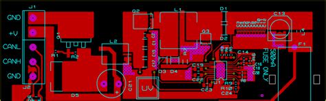
 Power-Distribution-ef6574bee47f11ee958ff7f8ca593eb4.jpeg” alt=”” class=”wp-image-136″ srcset=”https://electronicmanufacturingservice.org/wp-content/uploads/2024/03/PCB-Power-Distribution-ef6574bee47f11ee958ff7f8ca593eb4.jpeg”>
Designing a Robust Power Distribution Network
Now that we’ve looked at common PDN problems and their solutions, let’s discuss some best practices for designing a reliable PDN from the start.
Planning the Power Distribution Early
Power distribution should be considered from the very beginning of a PCB design, not tacked on as an afterthought. A robust PDN requires careful planning of the placement and routing of all power-related components and conductors.
Some factors to consider during the planning phase:
- Supply voltage and current requirements of all components
- Location of power input connectors
- Placement of voltage regulators and high-current devices
- Partitioning of analog and digital sections
- EMI/EMC and thermal constraints
Following the IPC-2152 Standard
The IPC-2152 standard, “Standard for Determining Current-Carrying Capacity in Printed Board Design”, provides guidelines for sizing conductors to ensure reliability and safety.
IPC-2152 charts specify the required trace width for a given current, copper weight, temperature rise, and board thickness. Many PCB design tools include IPC-2152 calculators to help optimize trace widths.
Some key parameters from the IPC-2152 standard:
| Copper Weight (oz) | Trace Width (mil) | Current Capacity (A) |
|---|---|---|
| 0.5 | 10 | 0.5 |
| 0.5 | 50 | 1.0 |
| 1.0 | 10 | 0.7 |
| 1.0 | 50 | 1.4 |
| 2.0 | 10 | 1.0 |
| 2.0 | 50 | 2.0 |
Note that these values assume a 20°C temperature rise above ambient. Always consult the full IPC-2152 specs for your specific design requirements.
Using Dedicated Power and Ground Planes
Whenever possible, dedicate one or more inner layers of a multi-layer PCB as solid copper power and ground planes. This provides several benefits:
- Increases current-carrying capacity
- Reduces DC resistance and AC impedance
- Creates a low-inductance path for current flow
- Provides shielding between signal layers
- Acts as a large decoupling capacitor
To make the most of power/ground planes:
- Carefully place supply pins to minimize current density
- Avoid perforating planes with large cutouts
- Connect planes to supply vias using wide copper pours
- Specify a suitable dielectric thickness for capacitance
Proper Bypassing and Decoupling
Bypassing and decoupling capacitors are critical for providing low-impedance, local energy storage to ICs and preventing noise from propagating through the PDN.
The impedance of a capacitor varies with frequency:
- At low frequencies, a capacitor is an open circuit
- At high frequencies, a capacitor is a short circuit
- In between, the capacitor has its rated capacitance
This frequency dependence allows capacitors to filter out noise on the PDN. A combination of bulk, ceramic, and package-level capacitors are used to decouple over a wide frequency range.
Some guidelines for bypassing and decoupling:
- Place decoupling caps as close as possible to IC supply pins
- Use multiple caps in parallel to reduce total impedance
- Choose cap values to target expected noise frequencies
- Minimize loop inductance with short, wide traces
- Use package-level caps for high-frequency noise
Example decoupling capacitor network:
| Capacitor | Value | Placement |
|---|---|---|
| Bulk | 100uF | Near voltage regulator output |
| Ceramic | 0.1uF | Near groups of digital ICs |
| Package-level | 0.01uF | Directly on power pins of ICs |
Optimizing Via Placement and Sizing
Vias are an essential but often overlooked part of the PDN. Poorly placed or undersized vias can add significant resistance and inductance, degrading power integrity.
Some tips for optimizing vias:
- Place vias as close as possible to device pins
- Use multiple vias in parallel to decrease resistance
- Specify larger via diameters for high-current nets
- Use filled or plated vias to increase current capacity
- Avoid unnecessarily changing reference planes with vias
Example via sizes for different current requirements:
| Current | Via Diameter | Plating Thickness | Resistance |
|---|---|---|---|
| 1A | 10mil | 1mil | 1.8mΩ |
| 2A | 20mil | 1mil | 0.8mΩ |
| 5A | 50mil | 2mil | 0.2mΩ |
Simulating and Measuring the PDN
Modern PCBs are complex, multi-layered structures with many potential points of failure in the PDN. Careful simulation and measurement are essential for verifying power integrity before and after fabrication.
Pre-layout simulation allows designers to optimize the placement and routing of power distribution components. Some common analyses include:
- DC voltage drop from source to load
- AC impedance across frequency
- Current density and thermal rise
- Electromagnetic field interactions
Post-fabrication measurements provide real-world verification of the PDN performance. Some key measurements:
- DC resistance between supply and ground
- Ripple and noise on the power rails
- Transient response to load steps
- Thermal imaging to identify hot spots
By simulating and measuring the PDN at various stages, designers can identify and correct issues before they lead to field failures.

FAQ
What is a power distribution network (PDN)?
A: A power distribution network (PDN) consists of all the conductors and components on a PCB that are involved in delivering power from the sources to the loads. This includes power and ground planes, traces, vias, connectors, and passive components like capacitors and inductors.
What are the main goals of PDN design?
A: The main goals of PDN design are to provide a low-impedance path for power to flow from the sources to the loads, maintain the correct voltage levels at all loads, minimize noise and ripple on the power rails, and avoid excessive heat generation. A well-designed PDN is critical for ensuring signal integrity and reliability.
What is the difference between bypassing and decoupling capacitors?
A: Bypassing and decoupling capacitors serve similar purposes but at different scales. Decoupling capacitors are typically larger value (1uF-100uF) caps placed near voltage regulators or power entry points to filter low-frequency noise. Bypassing capacitors are smaller value (0.01uF-0.1uF) caps placed very close to individual ICs to shunt high-frequency noise. In practice, the terms are often used interchangeably.
How can I determine the right size for my power traces?
A: The current-carrying capacity of a trace depends on its width, thickness, and acceptable temperature rise. The IPC-2152 standard provides charts and formulas for determining the minimum trace width for a given set of parameters. Most PCB design tools include trace width calculators based on IPC-2152. When in doubt, consult with your fabrication vendor.
What are some common symptoms of PDN problems?
A: Some common symptoms of PDN issues include:
- Intermittent resets or glitches
- Excessive heat generation
- Electromagnetic interference (EMI)
- Ripple or noise on power rails
- Signal integrity issues
- Premature component failure
If you suspect a PDN issue, a thorough design review and testing can help identify the root cause.
Conclusion
Proper PCB power distribution is essential for the reliable operation of any electronic device. By understanding common PDN problems and following best design practices, engineers can ensure their products meet performance and reliability goals.
Some key takeaways:
- Plan the PDN early in the design process
- Use dedicated power and ground planes when possible
- Follow the IPC-2152 standard for sizing conductors
- Place bypassing and decoupling capacitors close to ICs
- Optimize via placement and sizing to minimize resistance
- Simulate and measure the PDN to verify performance
With careful attention to power integrity throughout the design cycle, you can avoid being caught asleep at the wheel and deliver a product that exceeds expectations.
No responses yet