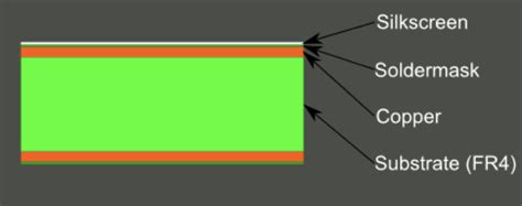
What is PCB Silkscreen?
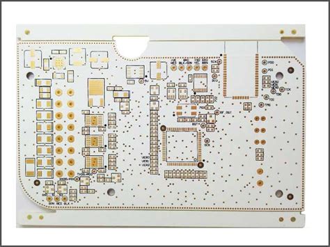
PCB silkscreen, also known as legend or nomenclature, is the layer of text and symbols printed on a printed circuit board (PCB) that provides important information about the board’s components, functions, and assembly. The silkscreen layer is typically white and is applied to the top and/or bottom surface of the PCB using a screen printing process.
The primary purpose of PCB silkscreen is to aid in the assembly, testing, and maintenance of the circuit board. It helps identify components, their orientation, and their values, making it easier for technicians and engineers to work with the board.
Common elements found on PCB silkscreen:
- Component labels (e.g., R1, C2, U3)
- Component values (e.g., 10k, 100nF, 74HC00)
- Polarity indicators (e.g., + and – for capacitors and diodes)
- Pin numbers for integrated circuits (ICs) and connectors
- Board revision number and date
- Company logo or product name
- Warning symbols or safety information
- Fiducial marks for automated assembly
Why is PCB Silkscreen Important?
PCB silkscreen plays a crucial role in the manufacturing, assembly, and maintenance of printed circuit boards. Here are some reasons why PCB silkscreen is important:
-
Assists in assembly: The silkscreen layer helps guide the placement of components during manual or automated assembly, reducing the chances of errors and improving the overall quality of the assembled board.
-
Facilitates troubleshooting: When a board malfunctions, the silkscreen information helps technicians quickly identify components and trace signals, making it easier to diagnose and fix issues.
-
Improves readability: A well-designed silkscreen layer enhances the readability of the PCB, making it easier for engineers and technicians to understand the board’s layout and functionality at a glance.
-
Provides valuable information: The silkscreen can include important information such as the board’s revision number, date of manufacture, and safety warnings, which can be helpful for tracking changes and ensuring proper handling of the board.
-
Enhances professional appearance: A clean and well-organized silkscreen layer gives the PCB a professional and polished look, which can be important for consumer products or presentations to clients.
How to Create DIY PCB Silkscreen
Creating a DIY PCB silkscreen is a relatively simple process that can be done using readily available materials and tools. Follow these steps to create your own PCB silkscreen:
Materials needed:
- PCB
- Laser printer
- Glossy photo paper
- Clothes iron
- Scissors or craft knife
- Isopropyl alcohol
- Cotton swabs
- Clear tape
Step 1: Design your silkscreen
- Use PCB design software (e.g., Eagle, KiCad, or Altium) to create your silkscreen layer.
- Ensure that the text and symbols are legible and properly oriented.
- Mirror the silkscreen design horizontally, as it will be transferred face-down onto the PCB.
- Print the mirrored silkscreen design onto glossy photo paper using a laser printer.
Step 2: Prepare the PCB
- Clean the PCB surface with isopropyl alcohol and a cotton swab to remove any dirt, grease, or residue.
- Allow the PCB to dry completely.
Step 3: Transfer the silkscreen
- Cut out the printed silkscreen design, leaving a small margin around the edges.
- Place the cut-out silkscreen face-down on the PCB, aligning it with the board’s features.
- Secure the silkscreen in place using clear tape.
- Set the clothes iron to its highest setting without steam.
- Place a piece of paper over the taped silkscreen to protect the iron.
- Press the iron firmly onto the paper for about 1-2 minutes, applying even pressure and heat across the entire surface.
Step 4: Remove the paper backing
- Allow the PCB to cool for a few minutes.
- Carefully peel off the tape and the photo paper backing.
- The toner from the laser printer should have transferred onto the PCB surface.
Step 5: Touch up and clean
- Use a fine-tipped permanent marker to touch up any imperfections or missing parts of the silkscreen.
- Clean the PCB with isopropyl alcohol to remove any residue or debris.
Your DIY PCB silkscreen is now complete! This method is suitable for small-scale or prototype PCBs, but for larger production runs or more complex designs, professional PCB manufacturing services are recommended.

Tips for Designing Effective PCB Silkscreens
When designing PCB silkscreens, there are several best practices to follow to ensure that the information is clear, legible, and useful. Here are some tips for designing effective PCB silkscreens:
-
Keep it simple: Use clear, concise labels and avoid clutter. Only include information that is necessary for assembly, testing, or maintenance.
-
Use appropriate font size and style: Choose a font that is easy to read, such as Arial or Helvetica, and ensure that the font size is large enough to be legible. A minimum font size of 0.8mm (0.032 inches) is recommended.
-
Maintain proper spacing: Provide adequate space between components and their labels to avoid confusion. A minimum spacing of 0.4mm (0.016 inches) between the silkscreen and other board features is recommended.
-
Avoid overlapping with other layers: Ensure that the silkscreen does not overlap with component pads, traces, or other critical board features, as this can lead to assembly errors or short circuits.
-
Use standard symbols and abbreviations: Employ commonly used symbols and abbreviations to make the silkscreen more easily understandable. For example, use “+” and “-” for polarity, “R” for resistors, “C” for capacitors, and “U” for integrated circuits.
-
Consider the assembly process: Place component labels and orientation marks in a way that facilitates the assembly process, whether manual or automated. Ensure that the labels are visible and not obstructed by the components themselves.
-
Include fiducial marks: For automated assembly, include fiducial marks on the silkscreen layer to help the pick-and-place machine align the board correctly.
-
Review and double-check: Before finalizing the silkscreen design, review it carefully for errors, inconsistencies, or omissions. Have a colleague or peer review the design as well to catch any issues that may have been overlooked.
By following these tips, you can create PCB silkscreens that are effective, informative, and professional-looking.
Advantages of DIY PCB Silkscreening
While professional PCB manufacturing services are recommended for large-scale production or complex designs, there are several advantages to creating DIY PCB silkscreens for small projects or prototypes:
-
Cost-effective: DIY silkscreening eliminates the need for expensive professional services, making it a cost-effective option for small-scale projects or hobbyists.
-
Quick turnaround: Creating a DIY silkscreen can be done in a matter of hours, allowing for faster iteration and testing of prototype designs.
-
Customization: With DIY silkscreening, you have complete control over the design and layout of the silkscreen, allowing for greater customization and flexibility.
-
Educational value: The process of creating a DIY silkscreen can be a valuable learning experience, helping you better understand the PCB manufacturing process and the importance of clear, well-designed silkscreens.
-
Accessibility: DIY silkscreening can be done with readily available materials and tools, making it accessible to a wide range of people, including students, hobbyists, and small businesses.
Frequently Asked Questions (FAQ)
-
Q: Can I use an inkjet printer instead of a laser printer for DIY PCB silkscreening?
A: No, inkjet printers are not suitable for this process because the ink does not transfer well to the PCB surface. Laser printers use toner, which can be heat-transferred to the PCB. -
Q: What should I do if the silkscreen doesn’t transfer properly to the PCB?
A: If the silkscreen doesn’t transfer well, try increasing the iron’s temperature or the duration of heat application. Ensure that the glossy photo paper is firmly pressed against the PCB surface and that there are no air bubbles or wrinkles. -
Q: Can I use this method for double-sided PCBs?
A: Yes, you can create DIY silkscreens for both sides of a double-sided PCB. However, be sure to align the silkscreens accurately on both sides to avoid confusion during assembly. -
Q: How durable is a DIY PCB silkscreen?
A: DIY silkscreens are not as durable as professionally applied silkscreens and may wear off over time, especially with frequent handling or exposure to solvents. For more durable silkscreens, consider using professional PCB manufacturing services. -
Q: Can I create multi-colored silkscreens using this method?
A: Creating multi-colored silkscreens using the DIY method is possible but more challenging. You would need to create separate silkscreen designs for each color and apply them to the PCB in stages, ensuring proper alignment and registration between the colors. For more complex, multi-colored silkscreens, professional services are recommended.
Conclusion
PCB silkscreening is an essential aspect of PCB design and manufacturing, providing valuable information for assembly, testing, and maintenance. While professional PCB manufacturing services are the best choice for large-scale production or complex designs, creating DIY PCB silkscreens can be a cost-effective and educational option for small projects or prototypes.
By following the steps outlined in this article and adhering to best practices for silkscreen design, you can create functional and professional-looking PCB silkscreens using readily available materials and tools. As you gain experience with DIY silkscreening, you’ll develop a better understanding of the PCB manufacturing process and be able to create more advanced and customized designs.
Remember to always prioritize clarity, legibility, and usefulness when designing your PCB silkscreens, and don’t hesitate to seek professional assistance for more complex or critical projects.
No responses yet