Introduction to Gerber-to-PCB Process
The process of converting Gerber Files into the data needed for printed circuit board (PCB) fabrication is a critical step in electronics manufacturing. This process, known as Design for Manufacturing (DFM), ensures that the PCB Design is optimized for manufacturability, reliability, and cost-effectiveness. In this article, we will explore the Gerber-to-PCB process in detail, covering everything from Gerber File Generation to the final production data used by PCB manufacturers.
What are Gerber Files?
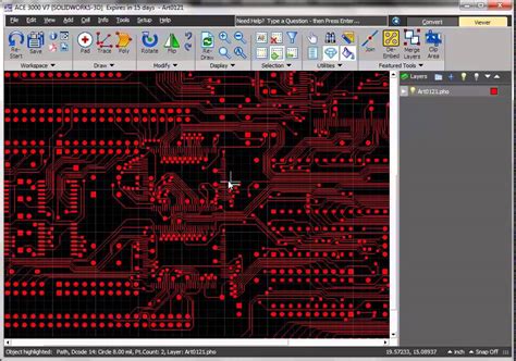
Gerber files are the standard format used to describe the layout of a PCB. They contain all the necessary information for PCB Fabrication, including the copper layers, solder mask, silkscreen, and drill data. Gerber files are generated by PCB design software, such as Altium Designer, Eagle, or KiCad, and are typically named with extensions that indicate their function, such as .GTL for top copper layer or .GBL for bottom copper layer.
Why is DFM Important?
DFM is crucial because it helps to identify and resolve any issues with the PCB design before it goes into production. By conducting a thorough DFM analysis, potential problems such as insufficient clearances, incorrect drill sizes, or missing solder mask can be caught and corrected early on. This not only saves time and money but also ensures that the final PCB meets all the necessary specifications and performs reliably in the field.
The Gerber-to-PCB Process
Step 1: Gerber File Generation
The first step in the Gerber-to-PCB process is generating the Gerber files from the PCB design software. This involves setting up the appropriate output settings, such as the file format (RS-274X), aperture lists, and layer mapping. It is essential to ensure that all the necessary layers are included and that the files are free of errors or inconsistencies.
Step 2: Gerber File Verification
Once the Gerber files have been generated, they need to be verified to ensure that they are complete and accurate. This can be done using specialized software tools that check for common issues such as missing apertures, overlapping traces, or incorrect pad sizes. Some popular Gerber file verification tools include:
- GC-Prevue
- ViewMate
- CAM350
Step 3: Panelization
For efficient production, multiple PCBs are often combined into a single panel. This process, known as panelization, involves arranging the individual PCBs on a larger board and adding tooling features such as fiducials, breakaway tabs, and registration holes. Panelization helps to minimize material waste, reduce handling time, and improve overall manufacturing efficiency.
Step 4: Tooling and Routing
Once the panel layout is finalized, the next step is to generate the tooling and routing data. This includes creating the drill files for hole sizes and locations, as well as the routing paths for the PCB outline and any internal cutouts. The tooling and routing data is typically output in a format compatible with the PCB manufacturer’s equipment, such as Excellon for drill files or Gerber for routing paths.
Step 5: Netlist and BOM Generation
In addition to the Gerber and tooling files, PCB manufacturers also require a netlist and bill of materials (BOM) for the assembly process. The netlist specifies the interconnections between components, while the BOM lists all the parts needed for the PCB Assembly. These files are usually generated from the PCB design software and provided along with the Gerber and tooling data.
Step 6: Final Data Package
The final step in the Gerber-to-PCB process is to package all the necessary files together for submission to the PCB manufacturer. This data package typically includes:
- Gerber files for each layer
- Drill files
- Routing files
- Netlist
- BOM
- Fabrication drawing or assembly instructions
It is important to ensure that all the files are properly named, formatted, and organized to avoid any confusion or delays in the manufacturing process.

Best Practices for Gerber-to-PCB
To ensure a smooth and successful Gerber-to-PCB process, follow these best practices:
- Use a consistent naming convention for your Gerber files, such as the IPC-356 standard.
- Include all the necessary layers in your Gerber output, including copper, solder mask, silkscreen, and drill data.
- Verify your Gerber files using a trusted software tool before submitting them for manufacturing.
- Optimize your panel layout for efficiency and cost-effectiveness, considering factors such as material utilization and tooling requirements.
- Provide clear and complete documentation, including a fabrication drawing and assembly instructions, to avoid any misunderstandings with the PCB manufacturer.

Conclusion
The Gerber-to-PCB process is a vital link in the electronics manufacturing chain, bridging the gap between PCB design and fabrication. By understanding the steps involved and following best practices for Gerber file generation, verification, and panelization, you can ensure that your PCB designs are efficiently and accurately translated into production-ready data. With a well-executed Gerber-to-PCB process, you can minimize errors, reduce costs, and accelerate your time-to-market for successful electronic products.

Frequently Asked Questions (FAQ)
1. What is the difference between Gerber files and ODB++ files?
Gerber files are the most widely used format for PCB fabrication data, containing information about individual layers such as copper, solder mask, and silkscreen. ODB++, on the other hand, is a more comprehensive data package that includes not only the layer information but also the netlist, component placement, and other design details. While Gerber files are still the industry standard, ODB++ is gaining popularity due to its enhanced capabilities for data exchange and design collaboration.
2. Can I use any PCB design software to generate Gerber files?
Yes, most PCB design software packages, including Altium Designer, Eagle, KiCad, and OrCAD, have the ability to generate Gerber files. However, the specific steps and settings for Gerber output may vary depending on the software being used. It is important to consult the software documentation or seek guidance from the vendor to ensure that you are generating Gerber files correctly and completely.
3. What should I do if my Gerber files fail the verification process?
If your Gerber files fail the verification process, it means that there are errors or inconsistencies that need to be addressed before proceeding with manufacturing. Common issues include missing layers, incorrect aperture sizes, or overlapping traces. To resolve these issues, carefully review the error report provided by the verification software and make the necessary corrections in your PCB design software. Re-generate the Gerber files and repeat the verification process until all errors are resolved.
4. How do I choose the right panel size for my PCB design?
Choosing the right panel size for your PCB design depends on several factors, including the dimensions of the individual boards, the quantity being produced, and the capabilities of the PCB manufacturer. In general, larger panel sizes offer better material utilization and lower cost per board, but may also require longer processing times and higher tooling costs. Smaller panel sizes provide more flexibility and faster turnaround times, but may be less cost-effective for high-volume production. It is best to consult with your PCB manufacturer to determine the optimal panel size for your specific project.
5. What is the typical turnaround time for PCB fabrication using Gerber files?
The turnaround time for PCB fabrication using Gerber files can vary depending on several factors, such as the complexity of the design, the quantity being produced, and the workload of the PCB manufacturer. For simple designs and standard specifications, turnaround times can be as short as 1-2 days for quick-turn prototyping services, or 5-7 days for regular production. For more complex designs or high-volume orders, turnaround times may extend to several weeks. It is important to communicate your timeline requirements clearly with the PCB manufacturer and plan accordingly in your project schedule.
No responses yet