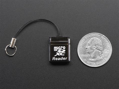
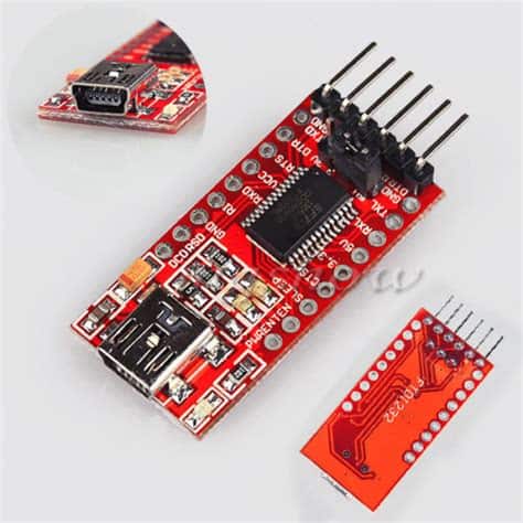
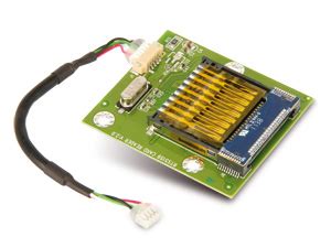
Why Build Your Own USB MicroSD Card Reader?
There are several reasons you may want to design and build your own USB MicroSD card reader:
- To learn about PCB design and fabrication
- To create a custom form factor to fit a specific enclosure or device
- As part of a larger project that requires MicroSD card functionality
- For fun and the satisfaction of building something yourself!
Building your own electronics, like a card reader, gives you full control and lets you customize it to your exact needs and specifications.
How USB MicroSD Card Readers Work
Key Components
A typical USB MicroSD card reader has the following main components:
| Component | Purpose |
|---|---|
| USB Connector | Connects reader to host device and provides power and data interface |
| MicroSD Socket | Socket that the MicroSD card plugs into |
| Card Detect Switch | Detects when a card is inserted or removed |
| Control IC | Integrated circuit that handles USB and MicroSD protocols and interfaces |
| Passives | Resistors, capacitors, etc. for power regulation, filtering, pull-ups/downs |
The USB connector and MicroSD socket are pretty self-explanatory – they are the physical interfaces for connecting the reader to a host computer and accepting a MicroSD card.
The card detect switch is used to signal to the control IC when a card has been inserted or removed, so it can mount or unmount the volume from the host operating system.
Control IC
The heart of the card reader is the control IC. This specialized chip handles all the complexities of implementing the USB and SD/MMC protocols and translating between them. Some popular choices are the Alcor AU6354 and the Genesys Logic GL823U.
These ICs have a USB interface on one side (usually USB 2.0 Full Speed) and an SD/MMC interface on the card side. They handle all the low-level details like:
- Negotiating USB enumeration with the host
- Receiving SCSI or BULK-ONLY MSC commands over USB
- Initializing the SD card and querying its properties
- Translating the USB commands into SPI or SDIO commands for the card
- Transferring data between the card and USB interface
- Monitoring card detect and write protect status
So you don’t need to worry about any of the USB or SD/MMC protocols in your design. You just need to supply the appropriate power rails, connect the IC’s USB data lines to your connector, hook up the SD interface to the card socket, and wire up the card detect switch. The IC takes care of the rest!

Schematic Design
Now that you understand the basic components and architecture of a USB MicroSD card reader, let’s dive into actually designing one!
Reference Schematic
The first step is to find the reference schematic for your chosen control IC in its datasheet. This will show you the recommended circuit for implementing it in a design. For example, here is the typical application circuit for the Genesys Logic GL823U:
You can use this as the starting point for your schematic. It shows the basic connections required, like:
- USB connector wired to IC’s USB+ and USB- pins
- MicroSD socket interfaces to IC’s SD_CLK, SD_CMD, SD_D0 pins
- Card detect switch between CD pin and ground
- 3.3V power and ground connections
- Decoupling capacitors on the power rails
Customizing the Schematic
Using the reference as a guide, you can now start creating your schematic in your preferred EDA tool (KiCad, Eagle, Altium, etc). You’ll want to make some changes and additions, like:
- Choosing the specific USB connector and MicroSD socket you want to use based on your mechanical requirements
- Adding a voltage regulator to produce the 3.3V rail if your USB power is 5V
- Putting a ferrite bead and bulk capacitor on VBUS for EMI suppression
- Adding mounting holes for mechanically securing the PCB
- Connecting an LED to the control IC if you want status indication
- Choosing values for the pull-up/down resistors and decoupling capacitors
Exactly what you’ll need to add will depend on the IC you’re using and your specific requirements. But after making these sorts of changes, you’ll have a complete schematic for your USB MicroSD card reader!

PCB Layout
Component Placement
With the finished schematic, you’re ready to start on the PCB layout. This is where you’ll arrange the physical components and route the copper traces that connect them.
The first step is placing the components. You’ll want to position the USB and MicroSD connectors on the edge of the board so they’re accessible. The control IC and other small components can go in the middle.
Refer to any mechanical drawings or models you have and make sure the port positions are correct. If the PCB will be fitting into an enclosure, you may have tight tolerances to meet.
Place the decoupling capacitors as close as possible to the power pins of the IC. This minimizes inductance and provides a low-impedance path for high-frequency noise.
Routing Guidelines
After placing components, you can route the copper traces between them. There are a few key considerations:
- Trace width: The USB data lines should be routed as a 90 ohm differential pair. This will likely require adjusting trace width and spacing compared to your defaults. The MicroSD and other low-speed signals can use your standard widths.
- Trace length: Keep the USB traces as short as possible to minimize reflections and signal integrity issues.
- Ground pour: Pour copper fills on the top and bottom layers and stitch them together with vias. This reduces EMI and provides a solid ground reference.
- Minimize crosstalk: Route the USB traces away from the MicroSD clock and data lines to avoid crosstalk.
Design Rule Checks
Before sending your board off for fabrication, make sure to run your EDA tool’s design rule checks (DRC). These will flag any potential errors or issues, like traces that are too close together or drill holes that are too small.
Some common checks to run include:
- Clearance: Ensures copper features are spaced far enough apart
- Trace width: Makes sure traces meet your specified minimum width
- Via size: Checks that vias are not too small to be drilled reliably
- Unconnected: Detects any traces that don’t connect to anything (usually accidental)
Carefully review any errors or warnings the DRC gives you and correct them in your design. Once the DRC passes, your board is ready for fabrication!

Fabrication and Assembly
Choosing a PCB Manufacturer
There are many PCB fabrication houses that can manufacture your design. Some popular ones include:
- JLCPCB
- PCBWay
- OSH Park
- Seeed Studio
Choose one based on your budget, lead time, and specific capabilities you need (like solder mask color or surface finish). Most fabs have an online quoting and ordering process where you upload your design files.
Ordering Components
In parallel with sending your PCB out for fabrication, you’ll also need to procure the components to assemble onto it. Refer to your schematic and bill of materials (BOM) to determine what parts you need.
Common component suppliers include:
- Digi-Key
- Mouser
- Arrow
- LCSC
Check stock and lead times to make sure you can get everything in time for when your PCB arrives. Consider ordering extras of inexpensive parts in case of assembly mistakes.
Soldering and Testing
With your PCB and components in hand, you’re ready for the fun part – soldering it all together! A few tips:
- Use a small tip on your soldering iron for the tiny surface mount parts
- Apply flux to help the solder flow and wet to the pads
- Work under magnification to see the details
- Take breaks to avoid getting fatigued and making mistakes
- Double check your work for shorts or unsoldered pins
After assembly, it’s time for the moment of truth – plug it in and test it out! Use a multimeter to check for any shorts on the power rails first. Then connect the board to your computer and see if it enumerates as a USB mass storage device.
If it works, congratulations! You’ve just designed and built your own USB MicroSD card reader. If it doesn’t, don’t get discouraged. Troubleshooting and debugging are valuable skills to learn. Check all your solder joints, review the schematic and layout, and methodically isolate the issue.
Frequently Asked Questions
What tools do I need to design a PCB?
To design a PCB like this USB MicroSD card reader, you will need:
- An EDA (electronic design automation) tool for schematic capture and PCB layout. Popular options are KiCad (free), Eagle, and Altium.
- A soldering iron, solder, and basic hand tools for assembly.
- A multimeter for testing and debugging.
- Technically you could design a PCB with just paper and pencil, but using an EDA tool is far easier and enables advanced features like design rule checking and autorouting.
How much does it cost to fabricate a PCB?
The cost to fabricate a PCB depends on several factors:
- Size: Larger boards are more expensive.
- Number of layers: Each additional copper layer adds cost.
- Quantity: Higher volumes have a lower per-unit cost.
- Turnaround time: Faster fabrication is more expensive.
- Special requirements: Tight tolerances, unusual materials, or additional manufacturing steps will increase cost.
As a rough ballpark, you can get small PCBs fabbed for around $5-20 each in low quantities, or under $1 in volume. The components to assemble onto the board are extra. Get quotes from several manufacturers for your specific design to compare.
What should I do if my assembled board doesn’t work?
First, don’t panic! Troubleshooting is part of the process. Here are some steps to take:
- Visually inspect the board for any obvious issues like unsoldered pins, cold solder joints, or damaged components.
- Use a multimeter to check for shorts between power and ground. A low resistance could indicate a short.
- Check that you have the correct voltage on the power rail.
- Use a multimeter or oscilloscope to probe test points and compare to expected values from the schematic.
- Review your schematic and layout for any design errors.
- Research your specific symptoms online – chances are someone else has encountered a similar issue!
- If all else fails, consider asking for help on forums or re-fabricating the board.
Remember, every troubleshooting challenge is an opportunity to learn and improve your skills!
Summary
Designing and building your own USB MicroSD card reader is a great electronics project. It involves skills like:
- Selecting components and creating a schematic
- Laying out a PCB and having it manufactured
- Sourcing parts and assembling the board
- Testing, troubleshooting, and debugging
While it may seem daunting at first, tackling a project like this is very rewarding. And after your first successful board spin, you’ll have the confidence to design ever more complex and ambitious PCBs!
So go ahead and give it a try. With some patience and persistence, you’ll soon have your own custom USB MicroSD card reader to show off. Happy designing!

No responses yet