Introduction to RF MEMS switches
Radio Frequency Microelectromechanical Systems (RF MEMS) switches have gained significant attention in recent years due to their superior performance compared to traditional solid-state switches. RF MEMS switches offer low insertion loss, high isolation, and excellent linearity, making them ideal for various applications in wireless communication systems, such as mobile phones, satellite communications, and radar systems.
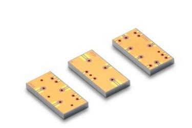
The integration of RF MEMS switches on printed circuit boards (PCBs) has become increasingly popular as it allows for cost-effective and scalable production of high-performance RF systems. However, the design and fabrication of RF MEMS switches on PCBs present several challenges that must be addressed to ensure reliable and efficient operation.
Key Considerations for RF MEMS Switch Design on PCBs
Substrate Selection
The choice of substrate material is crucial for the performance of RF MEMS switches on PCBs. The substrate must have low dielectric loss, high thermal stability, and good mechanical properties to support the MEMS structures. Some commonly used substrate materials for RF MEMS switches include:
- High-resistivity silicon (HR-Si)
- Fused silica
- Alumina (Al2O3)
- Low-temperature co-fired ceramic (LTCC)
Each substrate material has its advantages and disadvantages, and the selection depends on the specific requirements of the application, such as frequency range, power handling capability, and cost.
Actuator Design
The actuator is the heart of an RF MEMS switch, responsible for the mechanical movement that opens and closes the switch contacts. There are two main types of actuators used in RF MEMS switches:
- Electrostatic actuators
- Thermal actuators
Electrostatic actuators are the most common type, as they offer fast switching speed, low power consumption, and simple fabrication. However, they require high actuation voltages (typically 20-80 V) and are sensitive to dielectric charging effects. Thermal actuators, on the other hand, offer lower actuation voltages but have slower switching speeds and higher power consumption.
The design of the actuator must take into account the required actuation force, displacement, and reliability. Finite element analysis (FEA) tools are often used to optimize the actuator geometry and minimize stress concentrations.
Contact Design
The contact design is critical for the performance and reliability of RF MEMS switches. The contact materials must have low resistivity, high hardness, and good wear resistance to minimize contact resistance and ensure long-term reliability. Some commonly used contact materials include:
- Gold (Au)
- Ruthenium (Ru)
- Rhodium (Rh)
- Platinum (Pt)
The contact geometry also plays a significant role in the switch performance. The contact area should be large enough to minimize contact resistance but small enough to reduce the actuation force and improve switching speed. Various contact geometries, such as parallel plates, cantilevers, and membranes, have been used in RF MEMS switches.
Packaging and Hermetic Sealing
Packaging and hermetic sealing are essential for protecting the RF MEMS switches from environmental factors, such as humidity, dust, and temperature fluctuations. Proper packaging also helps to minimize the effects of parasitic capacitances and inductances on the switch performance.
Several packaging techniques have been developed for RF MEMS switches on PCBs, including:
- Wafer-level packaging (WLP)
- Chip-scale packaging (CSP)
- Thin-film encapsulation (TFE)
Hermetic sealing is typically achieved using materials such as glass, silicon, or ceramic, which provide a moisture-resistant barrier around the MEMS structures. The choice of packaging and sealing technique depends on the specific requirements of the application, such as the operating environment, frequency range, and cost.

Fabrication Process for RF MEMS Switches on PCBs
The fabrication process for RF MEMS switches on PCBs involves several steps, including:
- Substrate preparation
- Deposition of conductive and dielectric layers
- Patterning of MEMS structures
- Sacrificial layer etching
- Packaging and sealing
Substrate Preparation
The substrate preparation step involves cleaning the PCB surface and creating a smooth, flat surface for the deposition of the MEMS layers. This may involve chemical-mechanical polishing (CMP) or other planarization techniques to remove any surface irregularities.
Deposition of Conductive and Dielectric Layers
The conductive and dielectric layers are deposited on the prepared substrate using various techniques, such as sputtering, evaporation, or chemical vapor deposition (CVD). The conductive layers, such as gold or aluminum, form the switch contacts and interconnects, while the dielectric layers, such as silicon dioxide or silicon nitride, provide electrical insulation and mechanical support.
Patterning of MEMS Structures
The MEMS structures, including the actuator and contact elements, are patterned using photolithography and etching techniques. This involves applying a photoresist layer, exposing it to a patterned light source, and developing the resist to create a mask for selective etching of the underlying layers. Dry etching techniques, such as reactive ion etching (RIE) or deep reactive ion etching (DRIE), are commonly used for high-aspect-ratio structures.
Sacrificial Layer Etching
The sacrificial layer, typically made of silicon dioxide or photoresist, is used to create gaps and spaces between the MEMS structures and the substrate. After the MEMS structures are patterned, the sacrificial layer is selectively removed using wet or dry etching techniques, such as hydrofluoric acid (HF) etching or oxygen plasma etching. This releases the movable parts of the MEMS switch and allows for their free movement.
Packaging and Sealing
The final step in the fabrication process is packaging and sealing the RF MEMS switches to protect them from environmental factors. This may involve wafer-level packaging techniques, such as bonding a cap wafer to the MEMS wafer, or chip-scale packaging techniques, such as encapsulating the individual MEMS devices. Hermetic sealing is achieved using materials such as glass frit or metal alloys, which are bonded to the substrate and MEMS structures using thermal compression or anodic bonding techniques.

Challenges and Future Trends in RF MEMS Switch Fabrication on PCBs
Despite the significant progress made in the design and fabrication of RF MEMS switches on PCBs, several challenges still need to be addressed to ensure their widespread adoption and commercialization. Some of these challenges include:
-
Reliability and lifetime: RF MEMS switches must demonstrate reliable operation over billions of cycles and withstand various environmental factors, such as temperature fluctuations, humidity, and vibrations.
-
Packaging and sealing: Effective packaging and hermetic sealing techniques are crucial for protecting the MEMS structures and ensuring long-term reliability. However, the packaging and sealing processes can be complex and costly, especially for high-volume production.
-
Integration with other components: RF MEMS switches must be seamlessly integrated with other components on the PCB, such as antennas, filters, and amplifiers. This requires careful design and optimization of the interconnects and transitions between the MEMS and non-MEMS components.
-
Cost and scalability: The fabrication of RF MEMS switches on PCBs must be cost-effective and scalable to meet the demands of high-volume production. This requires the development of standardized processes and materials that can be easily adapted to different applications and substrates.
To address these challenges, researchers and industry experts are exploring various strategies and technologies, such as:
-
Advanced materials: The development of new materials, such as graphene or carbon nanotubes, may offer improved mechanical and electrical properties for RF MEMS switches, leading to higher reliability and performance.
-
3D printing: The use of 3D printing techniques, such as stereolithography or selective laser sintering, may enable the rapid prototyping and fabrication of complex MEMS structures on PCBs, reducing the time and cost of development.
-
Wafer-level packaging: The adoption of wafer-level packaging techniques, such as through-silicon vias (TSVs) or redistribution layers (RDLs), may simplify the packaging and integration of RF MEMS switches on PCBs, improving the overall system performance and reliability.
-
Standardization: The development of industry standards and guidelines for the design, fabrication, and testing of RF MEMS switches on PCBs may facilitate their widespread adoption and interoperability across different applications and platforms.
As these technologies and strategies continue to evolve, we can expect to see significant improvements in the performance, reliability, and cost-effectiveness of RF MEMS switches on PCBs, paving the way for their widespread use in various wireless communication systems.

Frequently Asked Questions (FAQ)
- What are the main advantages of RF MEMS switches over traditional solid-state switches?
-
RF MEMS switches offer several advantages over traditional solid-state switches, including:
- Low insertion loss: RF MEMS switches have a very low resistance when closed, resulting in minimal signal loss.
- High isolation: When open, RF MEMS switches provide excellent isolation between the input and output, minimizing signal leakage.
- High linearity: RF MEMS switches exhibit very low distortion, making them suitable for applications requiring high signal fidelity.
- Wide frequency range: RF MEMS switches can operate over a wide frequency range, from DC to millimeter-wave frequencies.
-
What are the main types of actuators used in RF MEMS switches?
-
The two main types of actuators used in RF MEMS switches are:
- Electrostatic actuators: These actuators use the attractive force between two charged plates to move the switch contacts. They offer fast switching speed and low power consumption but require high actuation voltages.
- Thermal actuators: These actuators use the expansion and contraction of materials due to temperature changes to move the switch contacts. They offer lower actuation voltages but have slower switching speeds and higher power consumption.
-
What are the key considerations for selecting a substrate material for RF MEMS switches on PCBs?
-
When selecting a substrate material for RF MEMS switches on PCBs, the following key considerations should be taken into account:
- Dielectric loss: The substrate should have low dielectric loss to minimize signal attenuation and maintain high-quality factor (Q) of the RF components.
- Thermal stability: The substrate should have good thermal stability to minimize the effects of temperature variations on the MEMS structures and maintain consistent performance.
- Mechanical properties: The substrate should have good mechanical properties, such as high stiffness and low stress, to support the MEMS structures and ensure reliable operation.
- Cost and availability: The substrate should be cost-effective and readily available to enable scalable production of RF MEMS switches on PCBs.
-
What are the main challenges in the fabrication of RF MEMS switches on PCBs?
-
The main challenges in the fabrication of RF MEMS switches on PCBs include:
- Reliability and lifetime: Ensuring reliable operation of RF MEMS switches over billions of cycles and under various environmental conditions is a significant challenge.
- Packaging and sealing: Developing effective packaging and hermetic sealing techniques that protect the MEMS structures while maintaining high performance and low cost is a complex task.
- Integration with other components: Seamlessly integrating RF MEMS switches with other components on the PCB, such as antennas and filters, requires careful design and optimization of interconnects and transitions.
- Cost and scalability: Achieving cost-effective and scalable fabrication of RF MEMS switches on PCBs to meet the demands of high-volume production is an ongoing challenge.
-
What are some of the future trends and technologies in RF MEMS switch fabrication on PCBs?
- Some of the future trends and technologies in RF MEMS switch fabrication on PCBs include:
- Advanced materials: Exploring new materials, such as graphene or carbon nanotubes, that offer improved mechanical and electrical properties for RF MEMS switches.
- 3D printing: Utilizing 3D printing techniques for rapid prototyping and fabrication of complex MEMS structures on PCBs, reducing development time and cost.
- Wafer-level packaging: Adopting wafer-level packaging techniques, such as through-silicon vias (TSVs) or redistribution layers (RDLs), to simplify the packaging and integration of RF MEMS switches on PCBs.
- Standardization: Developing industry standards and guidelines for the design, fabrication, and testing of RF MEMS switches on PCBs to facilitate their widespread adoption and interoperability across different applications.
No responses yet