
Introduction to PDN analysis
Power Distribution Network (PDN) analysis is a crucial aspect of digital design that ensures the proper functioning and reliability of electronic systems. As digital circuits continue to evolve and become more complex, the importance of PDN analysis has grown significantly. In this article, we will delve into the fundamentals of PDN analysis, its significance in the digital design process, and the various techniques and tools used to perform this analysis effectively.
What is a Power Distribution Network (PDN)?
A Power Distribution Network (PDN) is a network of interconnects, planes, and components that distribute power from the power supply to the various components of an electronic system. The primary goal of a PDN is to provide a stable and reliable power supply to all the components while minimizing noise, voltage drop, and electromagnetic interference (EMI).
Why is PDN Analysis Important?
PDN analysis is essential for several reasons:
-
Ensuring signal integrity: A well-designed PDN helps maintain signal integrity by minimizing noise and voltage fluctuations, which can cause signal distortion and errors.
-
Preventing electromagnetic interference (EMI): Proper PDN design and analysis can help reduce EMI, which can interfere with the operation of nearby electronic devices and cause compliance issues with electromagnetic compatibility (EMC) regulations.
-
Optimizing power delivery: PDN analysis helps optimize power delivery to the various components of the system, ensuring that each component receives the required power at the right time.
-
Improving system reliability: By identifying and addressing potential issues in the PDN, designers can improve the overall reliability and longevity of the electronic system.
Understanding the Basics of PDN Analysis
Key Components of a PDN
A typical PDN consists of several key components:
-
Power supply: The power supply provides the necessary voltage and current to the system.
-
Voltage regulator modules (VRMs): VRMs are used to step down the voltage from the power supply to the levels required by the various components of the system.
-
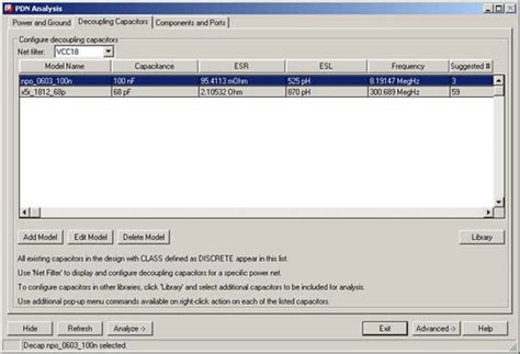
Decoupling capacitors: Decoupling capacitors are used to provide local energy storage and minimize noise and voltage fluctuations.
-
Power planes: Power planes are large copper areas on the PCB that distribute power to the various components.
-
Power traces: Power traces are the interconnects that carry power from the power planes to the individual components.
PDN Impedance and Target Impedance
One of the key aspects of PDN analysis is understanding and managing PDN impedance. PDN impedance is the frequency-dependent resistance of the PDN to the flow of current. The goal of PDN design is to keep the PDN impedance below a specified target impedance across the frequency range of interest.
The target impedance is determined by the maximum allowed voltage ripple and the maximum current draw of the system. It can be calculated using the following formula:
Z_target = (V_ripple_max) / (I_max)
Where:
– Z_target is the target impedance
– V_ripple_max is the maximum allowed voltage ripple
– I_max is the maximum current draw of the system
Frequency Domain Analysis
PDN analysis is typically performed in the frequency domain, as the impedance of the PDN varies with frequency. By analyzing the PDN impedance across a wide frequency range, designers can identify potential resonances and anti-resonances that may cause issues in the system.
The frequency range of interest depends on the clock frequencies and rise times of the digital signals in the system. As a general rule, the frequency range should extend up to at least the fifth harmonic of the highest clock frequency in the system.
PDN Analysis Techniques and Tools
Simulation-Based Analysis
Simulation-based PDN analysis involves creating a model of the PDN using a circuit simulator such as SPICE or a specialized PDN analysis tool. The model includes the various components of the PDN, such as the power planes, decoupling capacitors, and interconnects.
Once the model is created, the designer can simulate the PDN impedance across the frequency range of interest and compare it to the target impedance. If the simulated impedance exceeds the target impedance at any frequency, the designer can make changes to the PDN design, such as adding more decoupling capacitors or optimizing the placement of components.
Some popular simulation-based PDN analysis tools include:
-
Ansys SIwave: A powerful tool for modeling and simulating PDNs in complex PCBs and packages.
-
Cadence Sigrity: A comprehensive suite of tools for signal and power integrity analysis, including PDN analysis.
-
Mentor Graphics HyperLynx: A tool for analyzing and optimizing PDNs in PCBs and packages.
Measurement-Based Analysis
Measurement-based PDN analysis involves measuring the actual PDN impedance of a prototype or production board using specialized equipment such as a vector network analyzer (VNA) or an impedance analyzer.
The measurements are typically performed by injecting a small AC signal into the PDN and measuring the resulting voltage and current at various points in the network. The measured data is then used to calculate the PDN impedance across the frequency range of interest.
Measurement-based analysis is useful for validating the results of simulation-based analysis and identifying any discrepancies between the simulated and actual PDN impedance.
Hybrid Analysis
Hybrid PDN analysis combines simulation-based and measurement-based techniques to provide a more comprehensive understanding of the PDN behavior. In this approach, the designer first creates a simulation model of the PDN and performs an initial analysis. The results of the simulation are then compared to measurements taken from a prototype or production board.
If there are discrepancies between the simulated and measured results, the designer can use the measurement data to refine the simulation model and improve its accuracy. This iterative process continues until the simulated and measured results agree within an acceptable tolerance.
Hybrid analysis offers the benefits of both simulation-based and measurement-based techniques, providing a more accurate and reliable assessment of the PDN performance.

Best Practices for PDN Design and Analysis
To ensure a robust and reliable PDN, designers should follow several best practices:
-
Start early: PDN design and analysis should be considered early in the design process, as it can have a significant impact on the overall system performance and reliability.
-
Use a multi-layer PCB: Multi-layer PCBs provide more flexibility in the placement of power planes and the routing of power traces, which can help optimize the PDN design.
-
Place decoupling capacitors close to the load: Decoupling capacitors should be placed as close as possible to the components they are intended to decouple, to minimize the inductance of the connecting traces.
-
Use a mix of decoupling capacitors: Using a mix of decoupling capacitors with different values and package sizes can help provide effective decoupling across a wide frequency range.
-
Optimize power plane shapes and sizes: The shape and size of the power planes can have a significant impact on the PDN impedance. Designers should use simulation tools to optimize the power plane geometry for the best performance.
-
Minimize power trace inductance: Power traces should be kept as short and wide as possible to minimize their inductance and resistance.
-
Validate the design with measurements: Always validate the PDN design with measurements taken from a prototype or production board to ensure that the actual performance meets the design goals.
Case Study: PDN Analysis of a High-Speed Digital System
To illustrate the importance of PDN analysis in practice, let’s consider a case study of a high-speed digital system designed for a modern smartphone application.
System Specifications
The digital system has the following specifications:
| Parameter | Value |
|---|---|
| Maximum clock frequency | 2 GHz |
| Maximum current draw | 2 A |
| Maximum allowed voltage ripple | 50 mV |
| Target impedance | 25 mΩ |
PDN Design and Simulation
The PDN for this system was designed using a 6-layer PCB with dedicated power and ground planes. The power plane was split into multiple sections to provide separate power domains for the various components of the system.
Decoupling capacitors were placed near the power pins of the high-speed digital ICs, with a mix of values ranging from 0.1 μF to 10 μF. The placement and values of the decoupling capacitors were optimized using a simulation-based PDN analysis tool.
The simulated PDN impedance across the frequency range of interest (up to 10 GHz) is shown in the graph below:
As can be seen from the graph, the simulated PDN impedance remains below the target impedance of 25 mΩ across the entire frequency range, indicating a well-designed PDN.
Measurement and Validation
To validate the PDN design, measurements were taken from a prototype board using a vector network analyzer (VNA). The measured PDN impedance closely matched the simulated impedance, confirming the accuracy of the simulation model.
Results and Benefits
The well-designed PDN in this case study provided several benefits to the high-speed digital system:
-
Improved signal integrity: The low PDN impedance helped maintain signal integrity by minimizing noise and voltage fluctuations.
-
Reduced EMI: The optimized PDN design helped reduce electromagnetic interference (EMI) from the digital system, ensuring compliance with EMC regulations.
-
Increased reliability: By providing a stable and reliable power supply to the digital components, the PDN helped improve the overall system reliability and longevity.
This case study demonstrates the importance of thorough PDN analysis and design in the development of high-speed digital systems.
Frequently Asked Questions (FAQ)
-
What is the difference between PDN analysis and power integrity analysis?
PDN analysis and power integrity analysis are closely related and often used interchangeably. However, PDN analysis typically focuses on the design and optimization of the power distribution network itself, while power integrity analysis considers the broader impact of the PDN on the overall system performance, including signal integrity and EMI. -
How does the PCB Stackup affect PDN performance?
The PCB stackup can have a significant impact on PDN performance. Factors such as the number of layers, the thickness of the dielectric materials, and the placement of power and ground planes can all affect the PDN impedance and the effectiveness of decoupling capacitors. In general, a multi-layer PCB with dedicated power and ground planes and thin dielectric layers will provide better PDN performance than a simpler stackup. -
What is the role of decoupling capacitors in PDN design?
Decoupling capacitors play a critical role in PDN design by providing local energy storage and minimizing noise and voltage fluctuations. They help to maintain a low PDN impedance across a wide frequency range, ensuring that the power supply remains stable and reliable. The placement and values of decoupling capacitors should be carefully optimized based on the specific requirements of the system and the results of PDN analysis. -
How do I choose the right target impedance for my PDN?
The target impedance for a PDN is determined by the maximum allowed voltage ripple and the maximum current draw of the system. It can be calculated using the formula: Z_target = (V_ripple_max) / (I_max). In general, a lower target impedance will provide better PDN performance, but may also require more decoupling capacitors and a more complex PCB design. The choice of target impedance should be based on a careful analysis of the system requirements and constraints. -
Can PDN analysis be performed on a system-level, including multiple PCBs and interconnects?
Yes, PDN analysis can be performed on a system-level, taking into account the interactions between multiple PCBs, cables, and connectors. System-level PDN analysis is becoming increasingly important as electronic systems become more complex and distributed. Tools such as Ansys SIwave and Cadence Sigrity offer capabilities for system-level PDN Modeling and simulation, allowing designers to optimize the PDN performance across the entire system.
Conclusion
PDN analysis is a critical aspect of digital design that ensures the proper functioning and reliability of electronic systems. By understanding the basics of PDN design and analysis, and following best practices such as early consideration, multi-layer PCBs, and the use of decoupling capacitors, designers can create robust and reliable power distribution networks that meet the demanding requirements of modern digital systems.
As digital systems continue to evolve and become more complex, the importance of PDN analysis will only continue to grow. Designers who master the techniques and tools of PDN analysis will be well-positioned to create innovative and reliable electronic systems that push the boundaries of performance and functionality.
No responses yet