Introduction to the Cyclone Daughter Board
The DB31 Altera Cyclone II Daughter Board, also known as the Cyclone Daughter board, is a powerful and versatile development board designed for engineers, students, and hobbyists interested in FPGA (Field-Programmable Gate Array) technology. This board is built around the Altera Cyclone II FPGA, which offers a cost-effective solution for implementing complex digital logic designs.
What is an FPGA?
An FPGA is an integrated circuit that can be programmed and reprogrammed to perform various digital functions. Unlike traditional microprocessors or microcontrollers, which have fixed hardware architectures, FPGAs consist of a large array of configurable logic blocks (CLBs) that can be interconnected to create custom digital circuits. This flexibility allows designers to create highly optimized and application-specific hardware solutions.
Altera Cyclone II FPGA
The Altera Cyclone II FPGA is the heart of the DB31 Daughter Board. This FPGA family is designed for low-power, cost-sensitive applications, making it an ideal choice for a wide range of projects. Some key features of the Cyclone II FPGA include:
- Up to 68,416 logic elements (LEs)
- Up to 1.1 Mbits of embedded memory
- Up to 150 18×18 multipliers
- Up to 4 PLLs (Phase-Locked Loops)
- Support for various I/O standards (e.g., LVTTL, LVCMOS, SSTL, HSTL)
Hardware Overview of the DB31 Daughter Board
Board Layout and Components
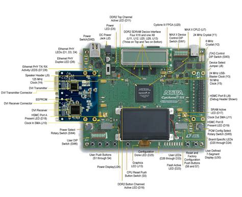
The DB31 Cyclone Daughter Board is designed to be compact and easy to use. The board measures approximately 10cm x 10cm and includes the following main components:
- Altera Cyclone II EP2C35F672C6 FPGA
- 32MB SDRAM
- 2MB Flash memory
- 50MHz oscillator
- USB-Blaster interface for programming and debugging
- Power supply circuitry (3.3V and 1.2V regulators)
- User I/O headers
- LEDs and push buttons for user interaction
Connecting the Daughter Board
The Cyclone Daughter Board can be connected to a host computer via the USB-Blaster interface, which provides both power and communication. The USB-Blaster allows you to program the FPGA, as well as debug your designs using tools like the Altera Quartus II software.
In addition to the USB-Blaster, the board also features user I/O headers that allow you to connect external peripherals or expansion boards. These headers provide access to various FPGA pins, enabling you to interface with sensors, actuators, displays, and other devices.

Getting Started with the Cyclone Daughter Board
Required Software and Tools
To start developing with the DB31 Cyclone Daughter Board, you will need the following software and tools:
- Altera Quartus II software (now called Intel Quartus Prime)
- USB-Blaster driver
- Verilog or VHDL for hardware description
- Optional: Nios II Embedded Design Suite for soft-core processor development
Installing the USB-Blaster Driver
Before you can program the FPGA or communicate with the Daughter Board, you must install the USB-Blaster driver on your host computer. The driver is typically included with the Altera Quartus II software, but you can also download it separately from the Altera website.
Creating a New Project in Quartus II
To create a new project in the Altera Quartus II software:
- Launch Quartus II and click on “New Project Wizard”
- Follow the wizard steps to specify your project name, location, and device family (Cyclone II)
- Select the specific device (EP2C35F672C6) and click “Finish”
Once your project is created, you can start designing your digital circuits using Verilog or VHDL.
Programming the FPGA
After you have completed your design and generated the programming file (.sof), you can program the FPGA on the Cyclone Daughter Board:
- Connect the board to your host computer via the USB-Blaster
- In Quartus II, select “Tools” > “Programmer”
- Click “Hardware Setup” and ensure the USB-Blaster is selected
- Click “Add File” and select your programming file (.sof)
- Check the “Program/Configure” box next to your file
- Click “Start” to begin the programming process
Once programming is complete, your design will be running on the FPGA.

Example Projects and Applications
Simple LED Blink
A great first project for the Cyclone Daughter Board is a simple LED blink example. This project demonstrates how to create a basic digital circuit that toggles an LED on and off at a fixed interval.
- Create a new project in Quartus II and select the Cyclone II device
- Create a new Verilog or VHDL file and write the code for a simple blink circuit
- Assign the LED pin to a user I/O header pin in the Pin Planner
- Compile the design and generate the programming file
- Program the FPGA and verify that the LED is blinking
VGA Display Controller
Another interesting project is a VGA display controller, which allows you to generate graphics and text on a standard VGA monitor.
- Create a new project and select the Cyclone II device
- Design a VGA controller module in Verilog or VHDL that generates the necessary timing signals (hsync, vsync, color)
- Create a framebuffer module to store the pixel data
- Instantiate the VGA controller and framebuffer modules in your top-level design
- Assign the VGA pins to the appropriate user I/O header pins
- Compile, generate the programming file, and program the FPGA
- Connect a VGA monitor to the Daughter Board and verify the display output
Nios II Soft-Core Processor
The Altera Cyclone II FPGA also supports the implementation of soft-core processors, such as the Nios II. A soft-core processor is a CPU that is implemented entirely in the FPGA fabric, providing a flexible and customizable processing solution.
To create a Nios II-based system on the Cyclone Daughter Board:
- Open Quartus II and launch the Qsys system integration tool
- Add a Nios II processor, memory interfaces, and any required peripherals to your system
- Generate the HDL files for your Qsys system
- Instantiate the Qsys system in your top-level Quartus II project
- Compile, generate the programming file, and program the FPGA
- Develop your software application using the Nios II Embedded Design Suite (EDS)
- Load and run your software on the Nios II processor using the EDS debugger

Troubleshooting and FAQs
1. What should I do if the USB-Blaster is not recognized by my computer?
First, ensure that you have installed the correct USB-Blaster driver. If the driver is installed but the device is still not recognized, try disconnecting and reconnecting the USB cable. If the issue persists, check if the USB port on your computer is functioning correctly by connecting another device.
2. My design compiles successfully but does not work when programmed onto the FPGA. What could be the problem?
There are several potential issues to consider:
- Check if your pin assignments are correct and match the actual connections on the Daughter Board
- Verify that your design meets the timing constraints and there are no timing violations
- Ensure that your design is properly synchronized and there are no metastability issues
- Double-check your Verilog or VHDL code for any logical errors or typos
3. How can I debug my design on the Cyclone Daughter Board?
You can use the SignalTap II Logic Analyzer, which is integrated into the Quartus II software, to debug your design. SignalTap II allows you to capture and analyze internal signals in your FPGA design during runtime. To use SignalTap II:
- Add the SignalTap II Logic Analyzer to your project
- Specify the signals you want to capture in the SignalTap II configuration
- Compile your design with SignalTap II enabled
- Program the FPGA and run the SignalTap II Logic Analyzer
- Trigger and capture the desired signals, then analyze the captured data
4. Can I use the Cyclone Daughter Board for real-time applications?
Yes, the Cyclone Daughter Board can be used for real-time applications, as FPGAs are known for their deterministic timing and low latency. However, you must ensure that your design meets the required timing constraints and that you have properly synchronized any external interfaces.
5. Are there any resources available for learning more about FPGA development with the Cyclone Daughter Board?
Yes, there are numerous resources available online for learning about FPGA development with the Cyclone Daughter Board and Altera FPGAs in general. Some recommended resources include:
- Altera (Intel) FPGA documentation and tutorials
- Online FPGA courses on platforms like Coursera, edX, and Udemy
- FPGA development forums, such as the Intel FPGA Forum and the EDA Board
- Books on FPGA development and digital design, such as “FPGA Prototyping by Verilog Examples” by Pong P. Chu and “Digital Design and Computer Architecture” by David Harris and Sarah Harris
Conclusion
The DB31 Altera Cyclone II Daughter Board is a powerful and versatile development platform for FPGA-based projects. With its Cyclone II FPGA, onboard memory, and user I/O headers, this board enables designers to create a wide range of digital systems, from simple blinking LEDs to complex soft-core processors and real-time applications.
By following the guidelines and examples provided in this article, you should be well-equipped to start exploring the world of FPGA development using the Cyclone Daughter Board. Remember to make use of the available resources, such as the Altera documentation, online forums, and educational materials, to further enhance your skills and knowledge in this exciting field.
Happy designing with the DB31 Altera Cyclone II Daughter Board!

No responses yet