The PCB Manufacturing Process: An Overview
The PCB manufacturing process can be broken down into several key stages:
- PCB Design and Layout
- PCB Fabrication
- PCB Assembly
- Testing and Quality Control
- Packaging and Shipping
Let’s dive into each of these stages in more detail.
PCB Design and Layout
The first step in the PCB manufacturing process is the design and layout of the circuit board. This is typically done using specialized software, such as Altium Designer or Eagle CAD.
Key Considerations in PCB Design
When designing a PCB, there are several key factors to consider:
- Component placement and orientation
- Trace width and spacing
- Power and ground planes
- Signal integrity and EMI (Electromagnetic Interference)
- Thermal management
PCB Layout Best Practices
To ensure optimal performance and reliability, it’s important to follow best practices when laying out a PCB:
- Use a grid system for component placement
- Keep traces as short and direct as possible
- Avoid sharp angles and use curved traces instead
- Use ground planes to minimize EMI
- Follow manufacturer guidelines for component footprints and pad sizes
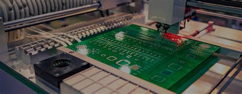
PCB Fabrication
Once the PCB design is finalized, it’s time to move on to the fabrication stage. This involves creating the physical circuit board from the digital design files.
PCB Fabrication Steps
The PCB fabrication process typically involves the following steps:
- Printing the circuit pattern onto a copper-clad laminate
- Etching away the unwanted copper to reveal the circuit traces
- Drilling holes for component leads and vias
- Applying a solder mask and silkscreen to the board
- Inspecting the board for defects and quality control
PCB Laminate Materials
PCBs can be fabricated using a variety of laminate materials, each with its own properties and characteristics:
| Material | Description | Typical Applications |
|---|---|---|
| FR-4 | Glass-reinforced epoxy laminate | General-purpose PCBs |
| Polyimide | High-temperature, flexible laminate | Aerospace and military applications |
| Teflon | Low-dielectric constant, high-frequency laminate | RF and microwave circuits |
| Aluminum | Metal-core laminate for high-power applications | LED lighting and power electronics |

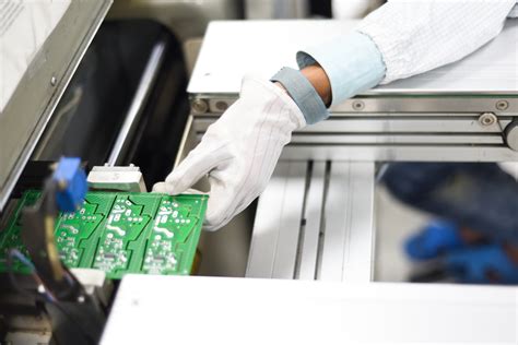
PCB Assembly
With the fabricated PCB in hand, the next step is to assemble the components onto the board. This can be done manually or using automated assembly equipment.
PCB Assembly Methods
There are two main methods for assembling PCBs:
- Through-hole assembly (THA): Components are inserted into holes drilled in the board and soldered in place.
- Surface-mount assembly (SMT): Components are placed directly onto pads on the surface of the board and soldered using reflow or wave soldering techniques.
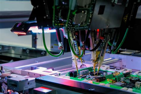
PCB Assembly Equipment
Automated PCB assembly relies on specialized equipment, such as:
- Pick-and-place machines for placing components onto the board
- Reflow ovens for soldering SMT components
- Wave soldering machines for soldering through-hole components
- Automated optical inspection (AOI) systems for quality control
Testing and Quality Control
Before a PCB can be shipped to the customer, it must undergo rigorous testing and quality control to ensure that it meets all specified requirements and functions as intended.
PCB Testing Methods
There are several methods used for testing PCBs:
- In-circuit testing (ICT): Probes are used to test individual components and circuits on the board.
- Functional testing: The board is powered up and tested to ensure that it performs its intended function.
- Boundary scan testing: A specialized test method for identifying faults in digital circuits.
- Burn-in testing: The board is subjected to elevated temperatures and voltages to identify early failures.
Quality Control Measures
In addition to testing, PCB manufacturers employ various quality control measures to ensure the consistency and reliability of their products:
- Visual inspection for defects and workmanship issues
- Statistical process control (SPC) to monitor and optimize the manufacturing process
- Traceability and record-keeping to track materials and processes used in each board
- Certification to industry standards such as ISO 9001 and IPC-A-610
Packaging and Shipping
Once the PCBs have passed all testing and quality control checks, they are ready to be packaged and shipped to the customer.
PCB Packaging Options
PCBs can be packaged in a variety of ways, depending on the customer’s requirements and the shipping method:
- ESD (electrostatic discharge) bags for protection against static damage
- Vacuum-sealed moisture barrier bags for protection against humidity
- Foam or bubble wrap for cushioning during shipping
- Pallets or crates for large orders or heavy boards
Shipping Methods
The choice of shipping method depends on factors such as the size and weight of the order, the destination, and the required delivery time:
- Courier services for small orders and fast delivery
- Freight carriers for large orders and international shipments
- Air freight for time-critical deliveries
- Ocean freight for large, heavy orders where cost is a primary concern
Frequently Asked Questions
What is the typical lead time for PCB manufacturing?
Lead times can vary depending on the complexity of the board, the fabrication process, and the manufacturer’s workload. Typical lead times range from a few days to several weeks.
How much does PCB manufacturing cost?
PCB manufacturing costs depend on factors such as the size and complexity of the board, the number of layers, the materials used, and the order quantity. Prices can range from a few dollars per board to several hundred dollars for complex, high-performance designs.
What are the most common PCB manufacturing defects?
Common PCB manufacturing defects include:
– Shorts and opens in circuit traces
– Incorrect component placement or orientation
– Solder bridges or insufficient solder on joints
– Damaged or missing components
– Contamination or corrosion on the board surface
How can I ensure the quality of my PCBs?
To ensure the quality of your PCBs, work with a reputable manufacturer that has a proven track record of quality and reliability. Provide clear and detailed specifications for your design, and communicate regularly with your manufacturer throughout the production process. Consider specifying industry standards such as IPC-A-610 for workmanship and quality control.
What should I look for in a PCB manufacturer?
When choosing a PCB manufacturer, consider factors such as:
– Experience and expertise in your industry or application
– Quality certifications and standards compliance
– Production capabilities and capacity
– Lead times and pricing
– Customer service and technical support
– Reputation and references from other customers
Conclusion
PCB manufacturing is a complex and multifaceted process that requires skill, precision, and attention to detail at every stage. From the initial design and layout to the final packaging and shipping, each step plays a critical role in ensuring the quality and reliability of the finished product.
By understanding the day-to-day operations of a PCB manufacturing facility, you can better appreciate the challenges and opportunities involved in bringing your electronic designs to life. Whether you’re a seasoned engineer or a newcomer to the world of PCBs, this comprehensive guide should provide a valuable overview of the key concepts and best practices in PCB manufacturing.
No responses yet