Introduction to PCB Packaging
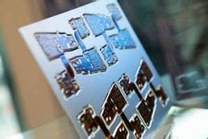
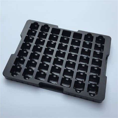
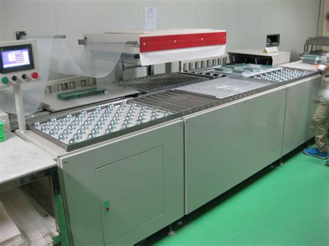
Printed circuit board (PCB) packaging is a critical aspect of electronics manufacturing that involves encasing and protecting the delicate components and circuits on a PCB. As electronic devices continue to become smaller, more powerful, and more complex, PCB packaging technology must keep pace to ensure reliability, performance, and cost-effectiveness. In this article, we’ll explore some of the cutting-edge technologies and trends in PCB packaging that are driving innovation in the electronics industry.
Advanced Packaging Techniques
System-in-Package (SiP)
System-in-Package (SiP) is an advanced packaging technique that involves integrating multiple integrated circuits (ICs) and other components into a single package. SiP offers several benefits over traditional PCB packaging, including:
- Reduced size and weight
- Improved performance and functionality
- Lower power consumption
- Simplified assembly and testing
SiP packages can be designed using various technologies, such as:
| Technology | Description |
|---|---|
| 2.5D packaging | Stacks multiple dies on an interposer with through-silicon vias (TSVs) |
| 3D packaging | Stacks multiple dies vertically with TSVs |
| Fan-out wafer-level packaging (FOWLP) | Embeds dies in a molding compound and redistributes the connections |
Embedded Die Packaging
Embedded die packaging is another advanced technique that involves embedding bare dies directly into the PCB substrate. This approach offers several advantages, such as:
- Reduced package size and thickness
- Improved electrical performance
- Enhanced thermal management
- Lower cost compared to traditional packaging
Embedded die packaging can be achieved using various methods, including:
| Method | Description |
|---|---|
| Chip-first | Dies are placed on the substrate before lamination |
| Chip-last | Dies are placed on the substrate after lamination |
| Chip-in-flex | Dies are embedded in a flexible substrate |
Wafer-Level Packaging (WLP)
Wafer-Level Packaging (WLP) is a packaging technique that involves packaging the dies while they are still on the wafer, before dicing. WLP offers several benefits, such as:
- Reduced package size and cost
- Improved electrical performance
- Higher manufacturing throughput
- Enhanced reliability
WLP can be implemented using various technologies, such as:
| Technology | Description |
|---|---|
| Fan-in WLP | Redistributes the connections within the die footprint |
| Fan-out WLP | Redistributes the connections beyond the die footprint |
| Through-silicon via (TSV) WLP | Creates vertical connections through the dies |

Advanced Materials
Low-Loss Dielectrics
Low-loss dielectrics are materials with low dielectric constant (Dk) and low dissipation factor (Df) that can improve the signal integrity and reduce the power loss in high-frequency PCBs. Some examples of low-loss dielectrics include:
- Polytetrafluoroethylene (PTFE)
- Liquid crystal polymer (LCP)
- Hydrocarbon ceramic (HCC)
- Polyphenylene oxide (PPO)
Low-loss dielectrics are particularly important for applications such as:
- 5G wireless communication
- Automotive radar
- High-speed data transmission
- Aerospace and defense
Thermal Interface Materials (TIMs)
Thermal Interface Materials (TIMs) are materials that facilitate the transfer of heat between the components and the heat sink or spreader in a PCB package. TIMs play a crucial role in ensuring the reliable operation and longevity of electronic devices by preventing overheating and thermal stress.
Some common types of TIMs include:
| Type | Description |
|---|---|
| Thermal greases | Silicone-based pastes filled with thermally conductive particles |
| Thermal pads | Elastomeric or phase-change materials with moderate thermal conductivity |
| Thermal adhesives | Epoxy or silicone-based adhesives with high thermal conductivity |
| Thermal gels | Silicone-based gels with low thermal resistance and high compliance |
The selection of TIMs depends on various factors, such as:
- Thermal conductivity
- Electrical insulation
- Mechanical properties
- Ease of application
- Cost
Advanced Substrates
Advanced substrates are materials with improved electrical, thermal, and mechanical properties that can enhance the performance and reliability of PCB packages. Some examples of advanced substrates include:
- High-density interconnect (HDI) substrates
- Copper-clad laminates (CCLs) with low Dk and Df
- Ceramic substrates with high thermal conductivity
- Metal-core PCBs (MCPCBs) with improved heat dissipation
Advanced substrates are particularly suitable for applications that require:
- High signal integrity
- Low power loss
- Effective thermal management
- Mechanical stability

Trends and Challenges
Miniaturization and High Density
One of the key trends in PCB packaging is the continuous miniaturization and increasing density of electronic components. This trend is driven by the demand for smaller, lighter, and more portable devices with enhanced functionality and performance.
However, miniaturization and high density also pose several challenges, such as:
- Signal integrity issues due to crosstalk and interference
- Thermal management difficulties due to limited space for heat dissipation
- Manufacturing complexity and cost due to smaller feature sizes and tighter tolerances
To address these challenges, PCB designers and manufacturers are adopting various strategies, such as:
- Using advanced packaging techniques like SiP and embedded die packaging
- Implementing low-loss dielectrics and advanced substrates
- Optimizing the layout and routing of the PCB
- Applying simulation and modeling tools to predict and mitigate potential issues
High-Speed and High-Frequency Applications
Another trend in PCB packaging is the increasing demand for high-speed and high-frequency applications, such as:
- 5G wireless communication
- Automotive radar and lidar
- High-performance computing
- Aerospace and defense
High-speed and high-frequency applications require PCB packages with:
- Low signal loss and distortion
- Controlled impedance and propagation delay
- Minimal electromagnetic interference (EMI)
- Adequate shielding and grounding
To meet these requirements, PCB designers and manufacturers are employing various techniques, such as:
- Using low-loss dielectrics and advanced substrates
- Implementing high-density interconnects (HDIs) and microvias
- Applying high-frequency laminate materials and coatings
- Optimizing the PCB stackup and via design
Environmental and Sustainability Concerns
As the electronics industry becomes more aware of its environmental impact, there is a growing emphasis on developing sustainable and eco-friendly PCB packaging solutions. This includes:
- Using halogen-free and lead-free materials
- Minimizing the use of hazardous substances
- Implementing recyclable and biodegradable packaging materials
- Adopting energy-efficient manufacturing processes
- Designing for ease of disassembly and recyclability
PCB manufacturers and suppliers are also working towards complying with various environmental regulations and standards, such as:
- Restriction of Hazardous Substances (RoHS) Directive
- Waste Electrical and Electronic Equipment (WEEE) Directive
- Registration, Evaluation, Authorization, and Restriction of Chemicals (REACH) Regulation

FAQ
1. What is the difference between SiP and embedded die packaging?
SiP involves integrating multiple ICs and components into a single package, while embedded die packaging involves embedding bare dies directly into the PCB substrate. SiP offers more flexibility in terms of component integration and can accommodate a wider range of die sizes and types. Embedded die packaging, on the other hand, offers a thinner profile and better electrical performance due to shorter interconnects.
2. What are the benefits of using low-loss dielectrics in PCB packaging?
Low-loss dielectrics can improve the signal integrity and reduce the power loss in high-frequency PCBs by minimizing the dielectric constant (Dk) and dissipation factor (Df). This results in lower signal attenuation, less distortion, and better overall performance. Low-loss dielectrics are particularly important for applications such as 5G wireless communication, automotive radar, and high-speed data transmission.
3. How do thermal interface materials (TIMs) help in PCB packaging?
TIMs facilitate the transfer of heat between the components and the heat sink or spreader in a PCB package. They help in ensuring the reliable operation and longevity of electronic devices by preventing overheating and thermal stress. The selection of TIMs depends on various factors, such as thermal conductivity, electrical insulation, mechanical properties, ease of application, and cost.
4. What are the challenges associated with miniaturization and high density in PCB packaging?
Miniaturization and high density in PCB packaging can lead to several challenges, such as signal integrity issues due to crosstalk and interference, thermal management difficulties due to limited space for heat dissipation, and manufacturing complexity and cost due to smaller feature sizes and tighter tolerances. To address these challenges, PCB designers and manufacturers are adopting various strategies, such as using advanced packaging techniques, implementing low-loss dielectrics and advanced substrates, optimizing the layout and routing of the PCB, and applying simulation and modeling tools.
5. Why is there a growing emphasis on environmental and sustainability concerns in PCB packaging?
As the electronics industry becomes more aware of its environmental impact, there is a growing emphasis on developing sustainable and eco-friendly PCB packaging solutions. This includes using halogen-free and lead-free materials, minimizing the use of hazardous substances, implementing recyclable and biodegradable packaging materials, adopting energy-efficient manufacturing processes, and designing for ease of disassembly and recyclability. PCB manufacturers and suppliers are also working towards complying with various environmental regulations and standards to reduce their environmental footprint and promote sustainability.
Conclusion
PCB packaging technology is continuously evolving to keep pace with the increasing demands for smaller, faster, and more reliable electronic devices. Advanced packaging techniques, such as SiP, embedded die packaging, and WLP, offer new ways to integrate and protect components while improving performance and functionality. Advanced materials, such as low-loss dielectrics, thermal interface materials, and advanced substrates, help in addressing the challenges associated with high-frequency and high-speed applications.
As the industry faces the trends of miniaturization, high density, and environmental sustainability, PCB designers and manufacturers must adopt innovative solutions and best practices to ensure the quality, reliability, and eco-friendliness of their products. By staying up-to-date with the latest technologies and trends in PCB packaging, electronics companies can gain a competitive edge and meet the ever-changing needs of their customers.

No responses yet