What is a Custom PCB?
A custom printed circuit board (PCB) is a bespoke electronic circuit designed and manufactured to meet specific requirements that aren’t served by generic, off-the-shelf PCBs. Custom PCBs offer several advantages:
- Tailored to exact specifications and functionality
- Optimized layout and component placement
- Proprietary design provides competitive advantage
- Cost-effective at volume production
Custom PCBs are used across industries in products like:
- Consumer electronics
- Industrial control systems
- Medical devices
- Automotive components
- Aerospace and defense applications
PCB Design Considerations
Designing a high-quality, reliable custom PCB requires careful planning and execution across several key areas:
Circuit Schematic
The circuit schematic forms the blueprint of the PCB, specifying components and connectivity. Best practices include:
- Use of standardized symbols and nomenclature
- Modular design with clear hierarchy
- Thorough annotation and cross-referencing
- Simulation and verification of circuit operation
Component Selection
Choosing the right components is critical to PCB performance, cost, and manufacturability. Consider:
- Functionality, specs, and tolerances
- Footprint and package type
- Availability and lead times
- Cost and minimum order quantities
- Compliance and certification requirements
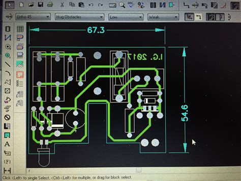
Board Layout
The component layout and routing determines the size, shape, layer count, and manufacturing complexity of the PCB. Optimize the layout for:
- Minimal size and layer count
- Efficient component placement
- Short, direct traces with minimal vias
- Proper grounding and shielding
- Accommodation of mechanical constraints
- Ease of assembly and rework
Manufacturability
Ensure the custom PCB design is practical and cost-effective to manufacture at scale by accounting for:
- Material selection (FR-4, aluminum, flex, etc.)
- Minimum trace width and spacing
- Drill hole sizes and via types
- Soldermask and silkscreen
- Surface finishes (HASL, ENIG, OSP, etc.)
- Testing and inspection requirements
PCB Manufacturing Process
The typical PCB manufacturing process involves the following steps:
-
Design review – Manufacturer analyzes design files (Gerber, drill, BOM) for completeness and manufacturability issues.
-
Material selection – Appropriate base materials, copper weights, and solder mask are selected based on PCB specifications.
-
Imaging – The circuit pattern is printed onto the copper-clad board using photoresist and UV exposure.
-
Etching – Exposed copper is chemically removed, leaving only the desired circuit traces.
-
Drilling – Holes are drilled for through-hole components and vias.
-
Plating – Drilled holes are plated with copper to provide electrical connectivity between layers.
-
Solder mask – An insulating layer is applied to protect the circuit, with openings for component pads and connections.
-
Silkscreen – Text and symbols are printed onto the board for component labels, branding, etc.
-
Surface finish – The exposed copper is coated to prevent oxidation and facilitate soldering. Popular finishes include:
| Finish | Composition | Advantages |
|---|---|---|
| HASL | Tin-lead | Low cost, easy to solder |
| ENIG | Nickel-gold | Flat surface, long shelf life |
| OSP | Organic compound | Inexpensive, no metals |
-
Singulation – The full PCB panel is cut into individual boards.
-
Quality control – Finished PCBs are inspected and tested to verify functionality and adherence to specifications.
Turnaround times for custom PCBs vary depending on complexity, material availability, and order quantity, but typically range from 1-2 weeks for prototypes to 4-6 weeks for production.

Design for Manufacturing (DFM)
Designing a custom PCB with manufacturing in mind from the start saves time, cost, and headaches down the line. Key DFM considerations include:
Board Specifications
Work with the manufacturer to determine optimal specs for:
- Board thickness
- Copper weight
- Number of layers
- Material grade
- Minimum hole size
- Surface finish
Clear communication of specs and expectations avoids costly rework later.
Panelization
PCBs are manufactured in large panels that are then cut into individual boards. Optimize panelization by:
- Minimizing waste material
- Allowing adequate spacing between boards
- Providing cut lines and fiducials
- Balancing panel utilization with assembly requirements
Component Placement
Careful component placement facilitates automated assembly and minimizes defects. Follow best practices such as:
- Consistent orientation
- Adequate spacing
- Proper polarity and alignment
- Consideration of assembly sequence
- Accommodation of test points
Clearances and Tolerances
Ensure the PCB design allows for sufficient clearances and tolerances in:
- Trace width and spacing
- Pad size and drill holes
- Soldermask and silkscreen
- Mechanical dimensions
Consult with the manufacturer on their specific capabilities and limits.
Assembly and Testing
Once the bare PCBs are manufactured, the next steps are assembly and testing to create a complete, functional product.
Assembly Methods
PCB assembly can be performed manually or with automated equipment depending on the complexity, quantity, and cost considerations. Common methods include:
-
Through-hole – Components are inserted into drilled holes and soldered on the opposite side. Suitable for large, heavy components, but more labor-intensive.
-
Surface mount (SMT) – Components are placed directly onto pads on the PCB surface and soldered using reflow ovens. Enables smaller, denser designs, but requires precise placement.
-
Mixed – A combination of through-hole and SMT components on the same board. Offers design flexibility but can increase assembly cost and complexity.
Soldering Techniques
Proper soldering is essential for reliable electrical and mechanical connections. The two main techniques are:
-
Wave soldering – The PCB is passed over a molten solder wave, coating the component leads and pads. Best suited for through-hole components.
-
Reflow soldering – Solder paste is applied to the pads, components are placed, and the board is heated to melt the solder. Used for SMT components.
Automated soldering provides consistency and throughput, while hand soldering allows for rework and prototyping.
Inspection and Testing
Thorough inspection and testing catch defects early and ensure the final product meets all functional and quality requirements. Common methods include:
-
Visual inspection – Manual or automated optical inspection of solder joints, component placement, and board condition.
-
Automated optical inspection (AOI) – High-speed camera system compares the assembled PCB to a reference image to detect defects.
-
X-ray inspection – Used to examine hidden solder joints, such as those under BGA components.
-
In-circuit testing (ICT) – Electrical testing of individual components and circuits using a bed-of-nails fixture.
-
Functional testing – Verifies the complete PCB operates as intended under various conditions and stimuli.
A comprehensive test strategy, tailored to the specific PCB design and application, maximizes coverage and minimizes escapes.
Frequently Asked Questions (FAQ)
1. How much does a custom PCB cost?
Custom PCB pricing depends on several factors, including:
- Board size and thickness
- Number of layers
- Material type
- Surface finish
- Quantity
In general, expect to pay $10-50 per board for small quantities (1-100), with significant price breaks at higher volumes. NRE (non-recurring engineering) costs for design and setup can add $500-5000 to the initial order.
2. What are the most common PCB materials?
The most widely used PCB material is FR-4, a glass-reinforced epoxy laminate. It offers good mechanical and electrical properties at a reasonable cost. Other common materials include:
- Aluminum for heat dissipation
- Polyimide for flexibility
- Rogers for high-frequency applications
- Ceramic for high-temperature environments
3. What file formats are needed for PCB manufacturing?
The primary file format for PCB manufacturing is Gerber, which contains the individual layer images and drill data. Other important files include:
- Bill of Materials (BOM) with component details
- Centroid file with component placement data
- Assembly drawings and instructions
Consult with the manufacturer on their specific file requirements and preferred formats.
4. How long does it take to get a custom PCB?
Turnaround times for custom PCBs vary depending on complexity, material availability, and order quantity. Typical lead times are:
- 1-2 weeks for prototypes
- 2-4 weeks for small production runs
- 4-8 weeks for large production runs
Rush services are often available for an additional fee, but may be limited by capacity and material constraints.
5. What certifications are important for PCB manufacturers?
When choosing a PCB manufacturer, look for relevant certifications such as:
- ISO 9001 for quality management
- UL 94 for flammability rating
- IPC Class 2 or 3 for workmanship standards
- RoHS for hazardous substance restriction
- ITAR for defense and military applications
Certifications demonstrate the manufacturer’s commitment to quality, reliability, and compliance with industry standards.
Conclusion
Creating a successful custom PCB requires careful consideration of design, manufacturing, assembly, and testing. By following best practices and working closely with experienced partners, you can bring your vision to life and create a high-quality, reliable product that meets your unique needs.
No responses yet