Introduction to Crystal Oscillators
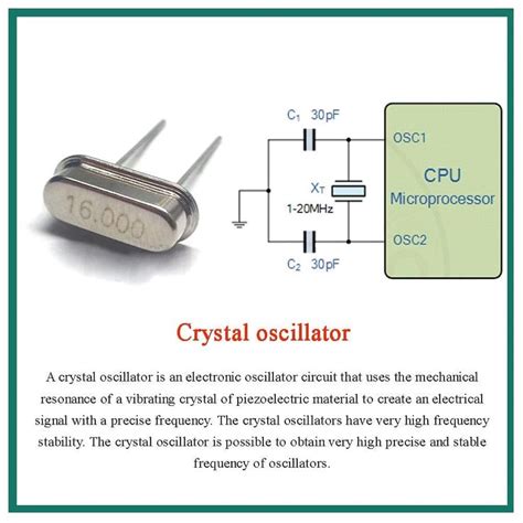
A crystal oscillator is an electronic circuit that uses the mechanical resonance of a vibrating crystal of piezoelectric material to create an electrical signal with a precise frequency. This frequency is often used to keep track of time, provide a stable clock signal for Digital Integrated Circuits, and to stabilize frequencies for radio transmitters and receivers.
What is a Crystal Oscillator?
A crystal oscillator is a type of electronic oscillator circuit that uses a quartz crystal as its frequency-determining element. The crystal acts as a highly stable and precise resonator, allowing the oscillator circuit to generate a periodic electronic signal with a very precise frequency.
The quartz crystal is a small, thin piece of quartz that has been precisely cut and shaped to vibrate at a specific frequency when an electric current is applied to it. The crystal’s frequency is determined by its size, shape, and the way it is cut.
Why Use a Crystal Oscillator?
Crystal oscillators are widely used in electronic devices because of their high stability, precision, and low cost compared to other types of oscillators. Some key advantages of crystal oscillators include:
-
High accuracy: Crystals can be manufactured to vibrate at a specific frequency with an accuracy of better than 100 parts per million (ppm).
-
Stability: The frequency of a crystal oscillator is highly stable over time and temperature variations.
-
Low noise: Crystal oscillators generate a very clean and pure signal with low phase noise.
-
Wide frequency range: Crystals can be cut to oscillate at frequencies ranging from a few kilohertz to hundreds of megahertz.
Applications of Crystal Oscillators
Crystal oscillators find applications in numerous electronic devices and systems, such as:
-
Timekeeping: Quartz watches and clocks rely on crystal oscillators for their accuracy.
-
Computer systems: Microprocessors and other digital integrated circuits use crystal oscillators to generate stable clock signals.
-
Communication systems: Radio transmitters and receivers use crystal oscillators to generate and stabilize carrier frequencies.
-
Instrumentation: Precise frequency references are essential for many types of scientific and industrial instrumentation.
Understanding the Crystal Oscillator Circuit
A crystal oscillator circuit consists of a quartz crystal and an amplifier, typically an inverting amplifier, connected in a positive feedback loop. The amplifier provides the necessary gain to overcome the losses in the crystal and maintain the oscillation.
Basic Crystal Oscillator Circuit
The most basic crystal oscillator circuit, known as the Pierce oscillator, is shown below:
            +---------+
           |         |
           |    +----|<---+
           |    |         |
          ---   |  Xtal   |
          ---   |         |
           |    +----|>---+
           |         |
           +---------+
In this circuit:
– The inverting amplifier is typically a single transistor or an inverter gate from a logic family such as CMOS or TTL.
– The crystal (Xtal) is connected between the input and output of the inverter, with optional capacitors in parallel for frequency tuning.
– The feedback resistor biases the inverter and provides DC feedback.
Series and Parallel Resonance
Quartz crystals have two resonant frequencies:
-
Series resonance: The frequency at which the crystal’s impedance is at its minimum and purely resistive. At this frequency, the crystal appears as a short circuit.
-
Parallel resonance: The frequency at which the crystal’s impedance is at its maximum and purely resistive. At this frequency, the crystal appears as an open circuit.
The parallel resonant frequency is slightly higher than the series resonant frequency. Most crystal oscillator circuits operate at the parallel resonant frequency.
Equivalent Circuit of a Crystal
A quartz crystal can be modeled as an equivalent electrical circuit, known as the Butterworth-Van Dyke (BVD) model:
            +---L---+
            |       |
      C     |  Cs   |    R
o-----||----+---||--+--/\/\/--o
            |       |
            +-------+
In this model:
– L represents the motional inductance
– Cs represents the motional capacitance
– R represents the loss resistance
– C represents the shunt capacitance (the capacitance of the electrodes and package)
The series combination of L, Cs, and R determines the series resonant frequency, while the parallel combination of L, Cs, R, and C determines the parallel resonant frequency.

Designing a Crystal Oscillator Circuit
When designing a crystal oscillator circuit, several factors need to be considered to ensure reliable operation and optimal performance.
Selecting the Crystal
The first step in designing a crystal oscillator is to select the appropriate crystal for the desired frequency and application. Crystals are specified by several parameters, including:
- Nominal frequency: The desired oscillation frequency.
- Frequency tolerance: The maximum deviation from the nominal frequency, usually expressed in parts per million (ppm) or percentage.
- Stability: The ability of the crystal to maintain its frequency over time and under varying conditions such as temperature and supply voltage.
- Load capacitance: The capacitance that the crystal is designed to work with for optimal performance.
Crystals are available in various packages, such as through-hole and surface-mount, and with different sizes and pin configurations.
Choosing the Amplifier
The amplifier in a crystal oscillator circuit must provide enough gain to overcome the losses in the crystal and maintain oscillation. The gain required depends on the crystal’s characteristics and the desired output signal level.
Common choices for the amplifier include:
- Discrete transistors: Bipolar junction transistors (BJTs) or field-effect transistors (FETs) can be used to build the inverting amplifier.
- Logic gates: Inverters from logic families such as CMOS or TTL can be used as the amplifier. The 74HCU04 unbuffered inverter is a popular choice.
- Dedicated oscillator ICs: Integrated circuits specifically designed for crystal oscillator applications, such as the CD4060 or the Si5351, can simplify the design process.
Oscillator Biasing
The oscillator amplifier must be biased correctly for reliable operation. The biasing should be designed to provide an amplifier gain higher than unity at the desired oscillation frequency while maintaining stability over temperature and supply voltage variations.
Biasing methods depend on the chosen amplifier:
- Discrete transistor circuits: Resistor-based biasing networks can be used to set the transistor’s operating point.
- Logic gate circuits: Most logic gates have limited drive capability and may require additional biasing components, such as pullup or pulldown resistors.
- Oscillator ICs: These often include internal biasing circuitry and may require minimal external components.
Load Capacitance and Frequency Tuning
The load capacitance seen by the crystal affects its oscillation frequency. Most crystals are designed to operate with a specific load capacitance, typically in the range of 10 to 30 pF.
The load capacitance includes the crystal’s shunt capacitance and any external capacitance, such as PCB stray capacitance and the input and output capacitance of the amplifier.
To ensure the oscillator operates at the desired frequency, the external load capacitance must be adjusted to match the crystal’s specified load capacitance. This is usually done by adding capacitors in parallel with the crystal.
The total load capacitance (CL) is given by:
CL = (C1 * C2) / (C1 + C2) + Cs
Where:
– C1 and C2 are the external capacitors
– Cs is the crystal’s shunt capacitance
Adjusting the values of C1 and C2 allows for fine-tuning of the oscillation frequency.
Output Buffering
The output signal from the crystal oscillator circuit may not be suitable for directly driving other circuits due to its limited drive capability and potential distortion. In such cases, an output buffer can be added to provide a clean, low-impedance output signal.
Output buffering options include:
- Discrete transistor stages: Additional transistor stages can be used to increase the output drive capability and improve signal quality.
- Logic gates: Unused gates from the same logic family as the oscillator amplifier can serve as output buffers.
- Dedicated buffer ICs: Integrated circuits designed for buffering and signal conditioning, such as the 74HC4050 or the 74HCU04, can be employed.

Building and Testing the Crystal Oscillator Circuit
With the design considerations in mind, we can now proceed to build and test the crystal oscillator circuit.
Step 1: Gather the Components
For this example, we will build a 10 MHz crystal oscillator using a 74HCU04 unbuffered inverter and a HC-49/U crystal package. The components required are:
- 74HCU04 Hex Inverter IC
- 10 MHz HC-49/U crystal
- 2x 18 pF ceramic capacitors
- 1 MΩ resistor
- 0.1 μF bypass capacitor
- Breadboard or PCB
- Power supply (5V)
Step 2: Assemble the Circuit
- Place the 74HCU04 IC on the breadboard or PCB.
- Connect the power supply (5V) to the VCC pin (pin 14) and ground to the GND pin (pin 7) of the IC.
- Place a 0.1 μF bypass capacitor between VCC and GND close to the IC.
- Connect the crystal between the input (pin 1) and output (pin 2) of one of the inverters.
- Connect an 18 pF capacitor between the inverter input and ground.
- Connect another 18 pF capacitor between the inverter output and ground.
- Connect a 1 MΩ resistor between the inverter input and VCC.
Step 3: Power Up and Test
- Apply power to the circuit.
- Use an oscilloscope to probe the output of the inverter (pin 2). You should see a clean, 10 MHz square wave signal.
- If the output signal is distorted or the oscillator fails to start, check your connections and component values.
- You can also measure the output frequency using a Frequency Counter to verify that it matches the crystal’s nominal frequency (10 MHz in this case).
Step 4: Optional Output Buffering
If you need to drive other circuits with the crystal oscillator output, you can use one or more of the remaining inverters in the 74HCU04 package as output buffers:
- Connect the input of an unused inverter to the output of the oscillator inverter.
- Use the output of this second inverter to drive external circuits.
- You can cascade multiple inverter stages for increased drive capability.

Troubleshooting and Optimization
Even with careful design and assembly, crystal oscillator circuits may sometimes fail to work as expected. Here are some common issues and their potential solutions:
Oscillator Not Starting
- Check the power supply voltage and ensure it is within the specified range for the amplifier and crystal.
- Verify that the crystal is connected correctly and that there are no shorts or open connections.
- Ensure the amplifier gain is sufficient to overcome the losses in the crystal. Try increasing the value of the feedback resistor or using a different amplifier.
- Check that the load capacitance seen by the crystal matches its specified value. Adjust the external capacitors if necessary.
Frequency Drift or Instability
- Ensure the crystal is operating within its specified temperature range. Consider using a temperature-compensated crystal oscillator (TCXO) for improved stability.
- Check for sources of noise or interference near the oscillator circuit, such as power supply ripple or digital switching noise. Use proper bypassing and decoupling techniques to minimize their impact.
- Verify that the oscillator circuit is not being overloaded by the external circuitry. Use appropriate output buffering and isolation techniques.
Spurious Oscillations or Harmonics
- Ensure the oscillator is not being driven into saturation or clipping. Reduce the amplifier gain or use a higher-speed amplifier if necessary.
- Check for parasitic resonances or coupling between the oscillator and other circuits. Use proper layout and shielding techniques to minimize these effects.
- Consider adding a low-pass or band-pass filter at the oscillator output to attenuate unwanted harmonics or spurious signals.
Crystal Damage or Aging
- Avoid exceeding the maximum drive level specified for the crystal, as this can cause overheating and permanent damage.
- Use crystals from reputable manufacturers and ensure they are handled and stored properly to minimize the risk of contamination or mechanical stress.
- Consider using crystal oscillator modules or temperature-compensated crystal oscillators (TCXOs) for applications that require long-term stability and reliability.
Conclusion
Crystal oscillators are essential building blocks in many electronic systems, providing precise and stable frequency references. By understanding the principles of crystal oscillator circuits and following proper design and assembly techniques, you can build reliable and high-performance oscillators for a wide range of applications.
Remember to consider factors such as crystal selection, amplifier design, load capacitance, and output buffering when designing your crystal oscillator circuit. Proper layout, grounding, and shielding are also crucial for optimal performance and stability.
With the knowledge gained from this article, you should be well-equipped to design, build, and troubleshoot crystal oscillator circuits for your projects. Happy oscillating!
Frequently Asked Questions (FAQ)
- What is the difference between a crystal oscillator and a ceramic resonator?
-
Crystal oscillators use a quartz crystal as the frequency-determining element, while ceramic resonators use a piezoelectric ceramic material. Crystals offer higher accuracy and stability than ceramic resonators but are more expensive and require more complex circuitry.
-
Can I use a crystal oscillator circuit to generate frequencies other than the crystal’s nominal frequency?
-
While crystal oscillators are designed to operate at the crystal’s nominal frequency, you can generate other frequencies by using frequency dividers or multipliers. However, the stability and accuracy of the resulting frequencies will depend on the quality of the frequency conversion circuitry.
-
How do I select the appropriate crystal for my application?
-
When selecting a crystal, consider factors such as the desired frequency, frequency tolerance, stability, and load capacitance. Consult the crystal manufacturer’s datasheets and application notes for guidance on choosing the right crystal for your specific requirements.
-
Can I use a crystal oscillator circuit to generate a sine wave output?
-
Crystal oscillator circuits typically produce square wave outputs. To generate a sine wave, you can use techniques such as filtering, waveform shaping, or using a dedicated sine wave generator IC. However, these methods may introduce additional complexity and potential sources of error.
-
How do I ensure the long-term stability of my crystal oscillator circuit?
- To ensure long-term stability, use high-quality crystals from reputable manufacturers and follow proper handling and storage procedures. Consider using temperature-compensated crystal oscillators (TCXOs) or oven-controlled crystal oscillators (OCXOs) for applications that require exceptional stability over wide temperature ranges. Regularly calibrate and maintain your oscillator circuits to minimize the effects of aging and drift.
No responses yet