Introduction to Copper PCBs and Common Concerns
Copper Printed Circuit Boards (PCBs) are an essential component in modern electronics. They provide the foundation for mounting and connecting electronic components to create functional devices. While copper PCBs offer many benefits such as good electrical conductivity, heat dissipation, and durability, users also have several common concerns when working with them.
In this article, we will explore 7 important issues that users are most concerned about when it comes to copper PCBs. We’ll discuss each concern in detail, provide examples and data to illustrate the issues, and offer potential solutions and best practices to address them. By the end, you’ll have a comprehensive understanding of the key concerns surrounding copper PCBs and how to mitigate them in your projects.
Concern 1: Copper Thickness and Its Impact on PCB Performance
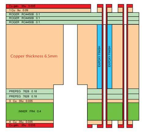
One of the primary concerns users have with copper PCBs is the thickness of the copper layer and how it affects the overall performance of the board. The copper thickness, measured in ounces per square foot (oz/ft²), plays a crucial role in determining the current carrying capacity, heat dissipation, and mechanical strength of the PCB.
Understanding Copper Thickness
Copper thickness is typically expressed in terms of weight per unit area, with 1 oz/ft² being the most common standard. This means that for every square foot of the PCB, there is 1 ounce of copper. The thickness can vary depending on the specific requirements of the project, with options ranging from 0.5 oz/ft² to 4 oz/ft² or more.
| Copper Thickness | Microns | Mils |
|---|---|---|
| 0.5 oz/ft² | 17.5 | 0.7 |
| 1 oz/ft² | 35 | 1.4 |
| 2 oz/ft² | 70 | 2.8 |
| 3 oz/ft² | 105 | 4.2 |
| 4 oz/ft² | 140 | 5.6 |
Impact on Current Carrying Capacity
The copper thickness directly affects the current carrying capacity of the PCB traces. Thicker copper layers can handle higher currents without overheating or suffering from voltage drops. This is particularly important for power-intensive applications or high-speed digital circuits.
To determine the appropriate copper thickness for your design, you need to consider factors such as the maximum current requirements, trace width, and temperature rise. Industry standards, such as IPC-2221, provide guidelines for calculating the current carrying capacity based on these parameters.
Impact on Heat Dissipation
Copper’s excellent thermal conductivity makes it an ideal material for dissipating heat generated by electronic components. A thicker copper layer enhances the PCB’s ability to spread and dissipate heat, reducing the risk of thermal issues and improving the overall reliability of the device.
When designing a PCB for heat-sensitive components, it’s essential to consider the copper thickness in conjunction with other thermal management techniques, such as using thermal vias, heat sinks, or copper pours.
Impact on Mechanical Strength
The copper thickness also contributes to the mechanical strength and rigidity of the PCB. Thicker copper layers provide better support for heavy components and enhance the board’s resistance to bending and warping.
However, it’s important to strike a balance between copper thickness and manufacturability. Excessively thick copper layers can pose challenges during the PCB fabrication process, such as difficulty in etching fine features or maintaining consistent plating thickness.
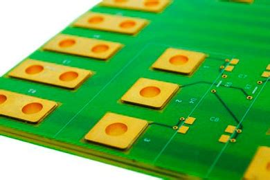
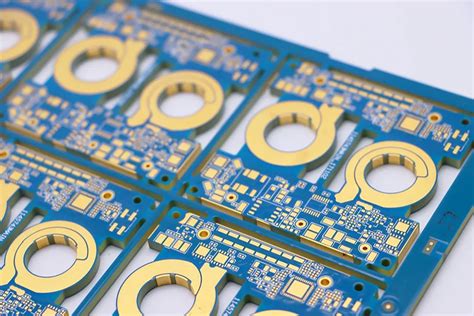
Concern 2: Copper Surface Finish and Solderability
Another significant concern for users of copper PCBs is the surface finish and its impact on solderability. The copper surface finish protects the exposed copper from oxidation and corrosion, while also providing a suitable surface for soldering components.
Common Copper Surface Finishes
There are several copper surface finishes available, each with its own advantages and limitations. Some of the most common finishes include:
-
Hot Air Solder Leveling (HASL): HASL involves dipping the PCB in molten solder and using hot air to remove excess solder, resulting in a thin, uniform layer of solder on the copper pads.
-
Electroless Nickel Immersion Gold (ENIG): ENIG consists of a layer of nickel plated onto the copper, followed by a thin layer of gold. This finish offers excellent solderability and shelf life.
-
Organic Solderability Preservative (OSP): OSP is a thin, organic coating applied to the copper surface to prevent oxidation. It provides good solderability but has a limited shelf life.
-
Immersion Silver (ImAg): ImAg involves plating a thin layer of silver onto the copper surface. It offers good solderability and is often used as a lower-cost alternative to ENIG.
| Surface Finish | Advantages | Limitations |
|---|---|---|
| HASL | – Cost-effective – Good solderability |
– Uneven surface – Limited fine-pitch compatibility |
| ENIG | – Excellent solderability – Long shelf life |
– Higher cost – Nickel corrosion (black pad) |
| OSP | – Low cost – Flat surface |
– Limited shelf life – Sensitive to handling |
| ImAg | – Good solderability – Lower cost than ENIG |
– Tarnishing over time – Possible silver migration |
Solderability Issues
Poor solderability can lead to various assembly issues, such as weak solder joints, bridging, or open connections. These issues can compromise the reliability and functionality of the final product.
To ensure good solderability, consider the following factors:
- Choose a suitable surface finish based on your project requirements, budget, and expected shelf life.
- Follow proper storage and handling procedures to prevent contamination or degradation of the surface finish.
- Use appropriate soldering techniques and parameters, such as temperature, time, and flux selection.
- Conduct solderability tests, such as wetting balance or surface insulation resistance (SIR) tests, to validate the quality of the surface finish.

Concern 3: Copper Trace Width and Spacing
The width and spacing of copper traces on a PCB are critical factors that users must consider to ensure proper signal integrity, manufacturability, and reliability.
Trace Width
The width of a copper trace determines its current carrying capacity and resistance. Wider traces can handle higher currents and have lower resistance, while narrower traces are more susceptible to overheating and voltage drops.
When deciding on trace widths, consider the following factors:
- Current requirements: Use industry standards, such as IPC-2221, to calculate the minimum trace width based on the expected current flow.
- Voltage drop: Ensure that the voltage drop across the trace is within acceptable limits to maintain proper circuit operation.
- Manufacturing capabilities: Consult with your PCB manufacturer to determine their minimum trace width capabilities and design guidelines.
Trace Spacing
The spacing between copper traces, also known as the clearance, is essential for preventing signal interference, crosstalk, and short circuits. Adequate trace spacing helps to maintain signal integrity and ensures reliable PCB performance.
When determining trace spacing, consider the following factors:
- Signal characteristics: High-speed or high-frequency signals require greater spacing to minimize crosstalk and maintain signal integrity.
- Voltage differences: Traces with large voltage differences should have increased spacing to prevent arcing or breakdown of the dielectric material.
- Manufacturing capabilities: Similar to trace width, consult with your PCB manufacturer to understand their minimum trace spacing capabilities and design rules.
| Trace Width/Spacing | Advantages | Limitations |
|---|---|---|
| Wide/Large | – Higher current capacity – Lower resistance |
– Increased board size – Higher manufacturing cost |
| Narrow/Small | – Smaller board size – Lower manufacturing cost |
– Lower current capacity – Higher resistance |
To optimize trace width and spacing, follow these best practices:
- Use PCB design software with built-in design rule checks (DRC) to ensure your layout meets the specified trace width and spacing requirements.
- Perform Signal integrity simulations to analyze the impact of trace width and spacing on signal quality and make necessary adjustments.
- Consider using controlled impedance techniques, such as stripline or microstrip, for critical high-speed traces to maintain consistent impedance and minimize signal reflections.
Concern 4: Copper Plating Thickness Variation
Inconsistent copper plating thickness across a PCB can lead to various issues, such as uneven current distribution, localized heating, and reduced reliability. Users are often concerned about the impact of copper plating thickness variation on the performance and longevity of their PCBs.
Causes of Copper Plating Thickness Variation
Several factors can contribute to variations in copper plating thickness, including:
- Uneven current distribution during the electroplating process, leading to thicker plating in some areas and thinner plating in others.
- Inadequate or inconsistent surface preparation, such as improper cleaning or activation of the copper surface before plating.
- Variations in the plating bath composition, temperature, or agitation, resulting in non-uniform plating deposition.
- Presence of contaminants or impurities in the plating bath, which can interfere with the plating process and cause thickness variations.
Impact of Copper Plating Thickness Variation
Uneven copper plating thickness can have several detrimental effects on PCB performance, such as:
- Localized heating: Areas with thinner plating may experience higher current densities and generate more heat, leading to localized hot spots and potential thermal issues.
- Reduced current carrying capacity: Thinner plating in some areas can limit the overall current carrying capacity of the traces, potentially causing voltage drops or overheating.
- Decreased reliability: Uneven plating thickness can result in weak points or stress concentrations, making the PCB more susceptible to mechanical failures or crack propagation.
To mitigate the impact of copper plating thickness variation, consider the following best practices:
- Work with reputable PCB manufacturers who have strict quality control processes and can provide consistent plating thickness across the board.
- Specify the acceptable range of plating thickness variation in your PCB design files and communicate these requirements clearly to your manufacturer.
- Request cross-sectional analysis or microsection testing of sample PCBs to verify the plating thickness uniformity and adherence to your specifications.
- Consider using thicker copper plating in critical areas, such as power traces or high-current paths, to provide an additional margin of safety against thickness variations.
Concern 5: Copper Trace Resistance and Voltage Drop
The resistance of copper traces and the resulting voltage drop are important concerns for users, as they can impact the performance and efficiency of the PCB and its associated circuitry.
Factors Affecting Copper Trace Resistance
The resistance of a copper trace depends on several factors, including:
- Trace length: Longer traces have higher resistance than shorter traces, assuming all other factors are equal.
- Trace width: Narrower traces have higher resistance than wider traces, as they offer less cross-sectional area for current flow.
- Copper thickness: Thinner copper layers result in higher trace resistance compared to thicker layers.
- Temperature: The resistance of copper increases with temperature, so traces exposed to higher temperatures will have increased resistance.
To calculate the resistance of a copper trace, you can use the following formula:
R = (ρ × L) / (W × T)
Where:
– R is the resistance (Ω)
– ρ is the resistivity of copper (Ω·m)
– L is the length of the trace (m)
– W is the width of the trace (m)
– T is the thickness of the copper layer (m)
Voltage Drop and Its Impact
Voltage drop occurs when current flows through a trace with finite resistance, resulting in a decrease in voltage along the length of the trace. This can have several consequences:
- Reduced voltage at the load: If the voltage drop is significant, the voltage delivered to the load (e.g., an IC or other component) may be insufficient for proper operation.
- Increased power dissipation: The power dissipated in the trace is equal to the product of the current and the voltage drop (P = I × ΔV). Higher voltage drops lead to increased power dissipation and potential thermal issues.
- Signal integrity issues: Voltage drops can cause signal degradation, particularly for high-speed or analog signals, leading to reduced noise margins or distortion.
To minimize voltage drop and its impact, consider the following strategies:
- Use wider traces for high-current paths to reduce resistance and voltage drop.
- Minimize trace lengths where possible to reduce overall resistance.
- Use thicker copper layers for power traces or other high-current paths to lower resistance.
- Perform voltage drop calculations during the design phase to ensure that the voltage delivered to each load is within acceptable limits.
- Consider using voltage regulation or compensation techniques, such as local voltage regulators or sense lines, to maintain proper voltage levels at critical loads.
Concern 6: Copper Pour and Grounding
Copper pour, also known as a ground plane or power plane, is a large area of copper on a PCB layer that is typically connected to ground or a power supply voltage. Users are often concerned about the proper use of copper pour and its impact on PCB performance and signal integrity.
Benefits of Copper Pour
Copper pour offers several advantages, including:
- Reduced impedance: A large area of copper connected to ground or power provides a low-impedance path for return currents, minimizing voltage fluctuations and improving signal quality.
- Improved EMI/EMC performance: Copper pour helps to shield sensitive signals from electromagnetic interference (EMI) and reduces the electromagnetic emissions from the PCB, contributing to better electromagnetic compatibility (EMC).
- Enhanced thermal management: Copper pour acts as a heat spreader, helping to distribute heat more evenly across the PCB and reducing localized hot spots.
- Increased mechanical stability: The added copper on the PCB layer enhances the mechanical strength and rigidity of the board, reducing the risk of warping or bending.
Grounding Strategies
Proper grounding is essential for ensuring reliable PCB performance and minimizing noise and signal integrity issues. When using copper pour for grounding, consider the following strategies:
- Use a dedicated ground plane: Assign one or more layers of the PCB exclusively for ground copper pour to provide a low-impedance return path for signals.
- Implement a star grounding topology: Connect all ground points to a central grounding location, such as a ground plane or a common ground point, to minimize ground loops and voltage differences.
- Avoid splitting ground planes: Maintain a continuous ground plane whenever possible, as splits or gaps can create impedance discontinuities and lead to signal integrity issues.
- Use stitching vias: Place vias at regular intervals to connect ground planes on different layers, ensuring a low-impedance path for return currents and minimizing voltage differences between layers.
Copper Pour Guidelines
When designing copper pour on your PCB, follow these guidelines to maximize its effectiveness:
- Maintain adequate clearance: Ensure that there is sufficient clearance between the copper pour and adjacent traces or components to prevent short circuits or signal coupling.
- Use hatched or cross-hatched patterns: Solid copper pour can cause issues during the PCB fabrication process, such as uneven etching or trapped gases. Using hatched or cross-hatched patterns allows for more even etching and improved manufacturability.
- Define pour keep-out areas: Specify keep-out areas where copper pour should not be present, such as around sensitive analog circuits or high-speed signals, to minimize interference and coupling.
- Connect copper pour to ground or power: Ensure that the copper pour is properly connected to the appropriate ground or power net using vias or traces to establish a low-impedance path.
Concern 7: Copper Trace Current Capacity and Ampacity
One of the critical concerns for users when designing copper PCBs is ensuring that the traces can handle the required current without overheating or suffering from excessive voltage drop. Understanding copper trace current capacity and ampacity is essential for creating reliable and efficient PCB designs.
Factors Affecting Current Capacity
The current carrying capacity of a copper trace depends on several factors, including:
- Trace width: Wider traces can handle higher currents than narrower traces, as they offer more cross-sectional area for current flow.
- Copper thickness: Thicker copper layers can carry more current than thinner layers, as they provide a larger cross-sectional area.
- Temperature rise: The maximum allowable current is limited by the acceptable temperature rise of the trace, which is influenced by factors such as ambient temperature, PCB material, and cooling mechanisms.
- Trace length: Longer traces experience a greater voltage drop and may require wider widths to maintain the same current capacity as shorter traces.
Ampacity Charts and Calculators
To determine the appropriate trace width for a given current requirement, designers often refer to ampacity charts or use online calculators. These resources provide guidelines for the maximum current a trace can carry based on its width, copper thickness, and acceptable temperature rise.
| Trace Width (mm) | 1
No responses yet