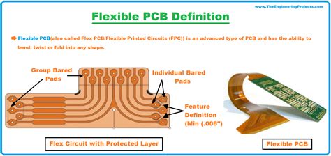
Introduction to Flexible PCBs and PCB Flex-Bending
Flexible printed circuit boards (PCBs) are a versatile alternative to traditional rigid PCBs. Unlike standard PCBs made from a solid substrate material, flexible PCBs use thin, bendable plastic films as the base material. This allows the PCB to be bent, twisted, and folded into a variety of shapes to fit into tight spaces or moving parts.
The ability to bend and flex the PCB opens up many possibilities for unique product designs and applications. Some key advantages of using flexible PCBs include:
- Reduced size and weight
- Increased reliability, as the PCB can flex with vibration and movement rather than crack
- Ability to fit PCBs into unconventional spaces and enclosures
- Dynamic movement of circuits for things like hinges, slides, and rotating joints
- 3D shaping of circuits
To take full advantage of a flexible PCB, the flex-bending capabilities need to be configured and in some cases animated through the design process. This article will dive into the key considerations and techniques for implementing PCB flex-bending.
Flexible PCB Materials and Layer Stack-Up
The foundation of any flexible PCB is the base material, which is typically a thin polymer film. Common materials used for flex PCBs include:
| Material | Typical Thickness | Key Properties |
|---|---|---|
| Polyimide | 1-5 mils | High heat resistance, most common |
| Polyester | 2-5 mils | Lower cost, good for dynamic flexing |
| Liquid Crystal Polymer | 1-4 mils | Very thin, high frequency performance |
In addition to the base substrate, flex PCBs are composed of one or more conductive layers of copper traces. Between each layer is an adhesive material to bond the layers together. And the outer layers are often coated with a protective coverlay.
A typical flexible PCB stack-up may look like this:
| Layer | Material | Thickness |
|---|---|---|
| Top Coverlay | Polyimide | 1 mil |
| Top Conductor | Copper | 0.5-1 oz |
| Adhesive | Acrylic | 1 mil |
| Base Film | Polyimide | 2 mil |
| Adhesive | Acrylic | 1 mil |
| Bottom Conductor | Copper | 0.5-1 oz |
| Bottom Coverlay | Polyimide | 1 mil |
The number of layers and specific materials can be adjusted based on the electrical and mechanical requirements. More layers allow for higher circuit density but will increase the thickness and decrease flexibility.
Designing Flexible Circuits for Bending
Bend Radius and Cycle Life
Two of the most important parameters to consider when designing a flex circuit for bending are the bend radius and flex cycle life:
-
Bend Radius – The bend radius refers to the minimum radius the PCB can be bent to without damaging the circuit. This is determined by the substrate and conductor materials and thicknesses. Typical minimum bend radii are 6-10 times the overall PCB thickness.
-
Flex Cycle Life – The number of times the PCB can be flexed before the conductors begin to crack and fail. This is mainly influenced by the copper thickness, with thinner conductors allowing for a longer flex life. The type of flexing motion (rolling vs. creasing) also impacts cycle life.
The following table shows the relationship between copper thickness and flex cycle life:
| Copper Thickness | Flex Cycles (Rolling) | Flex Cycles (Creasing) |
|---|---|---|
| 1/2 oz (18 um) | >2,000,000 | >500,000 |
| 1 oz (35 um) | 50,000-100,000 | 20,000-50,000 |
| 2 oz (70 um) | 200-500 | 50-100 |
To maximize the bend radius and flex cycle life, it’s best to use the thinnest possible conductors and adhesive layers. Adding strain relief such as slots or accordian folds at the flex points can also help.
Circuit Pattern and Trace Routing
The circuit pattern and how the copper traces are routed play a big role in the flexibility and reliability of the PCB. Some guidelines to follow include:
- Orient traces perpendicular to the bend axis to minimize stretching
- Avoid putting traces or pads directly on the bend area
- Use curved or angled traces rather than 90 degree bends
- Increase the trace width in flex zones to lower resistance and improve reliability
- Stagger traces and pads to distribute stress evenly
- Avoid plated through-holes in flex areas, use SMT components instead
Here’s an example of routing traces for good flexibility:
 Bend Axis
    ↓
 ───┬────────────┬───
    │ ╭────────╮ │
    │ │······  │ │
    │ │  ····│ │ │
    │ │  ││  │ │ │
    │ ╰──────│╯ │
    │     ╭──│──╮
    │     │  │  │
    │     ╰─────╯
 ───┴────────────┴───
Stiffeners and Rigidized Zones
In most cases, portions of the flex PCB will need to remain rigid to mount components or connectors. This is achieved by bonding stiffeners to one or both sides of the PCB in specific areas.
Stiffeners are commonly made from FR-4 glass epoxy, polyimide glass, or metal. The stiffener material and thickness should be selected based on the weight of the attached components and the desired level of rigidity.
Rigidized areas can be created by selectively laminating the PCB with a rigid material or by designing “rigid-flex” boards that selectively remove the adhesive layers between certain zones.

3D Modeling and Folding Simulation
To ensure the flexible PCB will fit and function as intended in the final assembly, it’s important to create a 3D model of the circuit and simulate its folding behavior. This allows you to check for potential issues like collisions, kinks, or excessive strain before committing to a physical prototype.
Most mechanical CAD tools have features for importing and manipulating PCB designs in 3D space. The flex circuit can be modeled as a thin sheet with assigned material properties. Then the folding and bending can be simulated using tools like collision detection, finite element analysis (FEA), and animation.
Some things to look for in the folding simulation include:
- Ensuring bend radii stay above the allowed minimum at all points
- Checking that stiffened areas end up in the correct positions
- Verifying that the PCB shape allows it to fold up as intended
- Identifying any potential pinch points or areas of high strain
- Confirming connectors and components do not interfere with the folding
It’s a good idea to simulate the full range of motion that the PCB will experience to weed out any design flaws or reliability risks. The 3D model can also be used to generate realistic visualizations and assembly instructions.

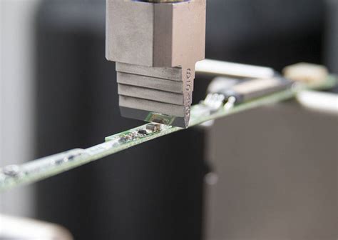
Prototyping and Testing
Once the design has been vetted through simulation, the next step is to produce physical prototypes for real-world testing. Due to their unique processing requirements, flex PCBs are usually prototyped and manufactured by specialized fabrication shops.
Some key aspects to discuss with the manufacturer include:
- Material selection and stack-up
- Minimum feature sizes and tolerances
- Controlled impedance and shielding requirements
- Specific areas for rigidization and stiffening
- Panelization and assembly preferences
It’s also important to clearly communicate the expected flexing and bending behavior of the circuit, as this will influence the fab and assembly approach. Providing the 3D model and folding simulation can be very helpful.
When the prototype boards arrive, they should be promptly inspected and tested:
- Carefully examine the boards for any manufacturing defects
- Check that the boards flex and fold as expected without damage
- Measure the bend radii and overall dimensions
- Perform electrical testing to verify connectivity and performance
- Assemble the PCBs into the full product enclosure
- Test the dynamic flexing behavior in the actual use case
- Assess the mechanical durability with cycle testing
Any issues discovered in the prototyping phase should be addressed through design revisions and discussions with the manufacturer. The testing results will help predict the reliability and lifespan of the flex circuit in the final product.
FAQs
What are some common applications for flex PCBs?
Flex PCBs are commonly used in:
- Wearables and consumer electronics
- Medical devices and implants
- Aerospace and military equipment
- Automotive electronics
- Industrial sensors and controls
How much do flexible PCBs cost compared to rigid boards?
In general, flex PCBs cost 20-50% more than rigid boards due to the specialized materials, processes, and tooling required. The exact cost premium depends on the circuit complexity, layer count, and order volume.
Are there any limitations on what components can be used on flex PCBs?
Most standard surface mount components can be used on flex PCBs, but larger or heavier parts may necessite stiffeners for mechanical support. Plated through-hole components should be avoided in dynamic flex zones. The assembly process also requires special tools and techniques to avoid damaging the boards.
What data is needed to get a flex PCB quote from a manufacturer?
Most flex PCB manufacturers will need:
- Material stack-up and expected thicknesses
- Conductor routing layers and data
- Outer dimensions and any cutouts or unusual shapes
- Rigidized areas and stiffeners
- Surface finish and markings
- Expected bend radii and flex cycle requirements
Can flexible PCBs be used for high-frequency RF circuits?
Yes, flex PCBs can be engineered for RF performance by using low-loss base materials, smooth copper finishes, and controlled impedance traces. However, the flexing behavior can impact RF performance, so the bending dynamics must be accounted for in the circuit design and simulation.
Conclusion
Flexible PCBs open up exciting design possibilities beyond the limitations of conventional rigid boards. By carefully configuring the stack-up, materials, and circuit pattern, flex PCBs can be engineered to bend and fold with high reliability.
3D modeling and folding simulation are key for assessing the dynamic mechanical behavior of flex circuits prior to manufacturing. And thorough prototyping and testing are needed to validate the actual bending performance.
With the proper design approach and manufacturing controls, product developers can take advantage of PCB flex-bending to enable new form factors and dynamic electronic applications.
No responses yet