The Importance of Clear PCB Stackup Communication
When designing a printed circuit board (PCB), one of the most crucial aspects is the layer stackup. The PCB stackup refers to the arrangement of copper layers, insulating materials, and other elements that make up the structure of the board. Effective communication of the PCB stackup requirements to the manufacturer is essential to ensure that the final product meets the desired specifications and performs as intended. In this article, we will discuss the importance of clear PCB stackup communication and provide guidance on how to effectively convey your needs to manufacturers.
Why PCB Stackup Communication Matters
-
Functionality: The PCB stackup directly impacts the functionality of the board. Factors such as layer thickness, dielectric properties, and copper weight can affect signal integrity, power distribution, and thermal management. Clear communication ensures that the manufacturer understands your requirements and can produce a board that meets your functional needs.
-
Manufacturability: Not all PCB stackups are easily manufacturable. Some designs may require specialized materials or processes that not all manufacturers can accommodate. By communicating your stackup needs upfront, you can ensure that the manufacturer has the capabilities to produce your board efficiently and cost-effectively.
-
Cost: The choice of materials, number of layers, and other stackup parameters can significantly impact the cost of the PCB. Clear communication helps the manufacturer provide accurate quotes and allows you to make informed decisions about trade-offs between cost and performance.
-
Reliability: The PCB stackup plays a crucial role in the reliability of the final product. Factors such as the choice of laminate materials, copper thickness, and via design can affect the board’s durability and long-term performance. By communicating your reliability requirements, you can ensure that the manufacturer selects appropriate materials and processes.
Key Elements of PCB Stackup Communication
When communicating your PCB stackup needs to manufacturers, it’s essential to provide comprehensive and clear information. Here are the key elements to include:
1. Number of Layers
Specify the total number of layers required for your PCB. This information helps the manufacturer determine the overall thickness of the board and select appropriate materials.
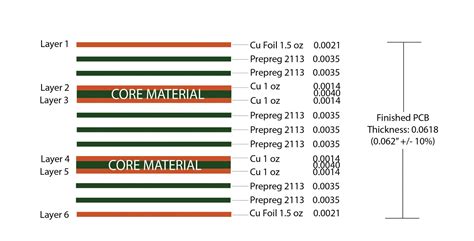
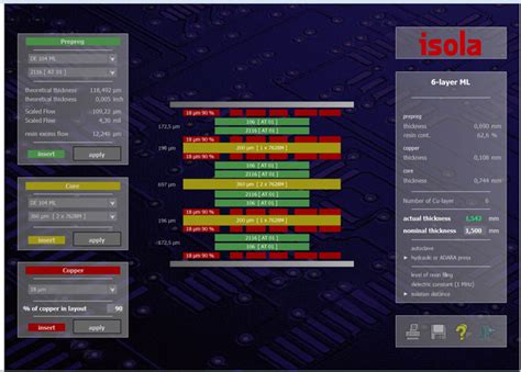
2. Layer Stack Diagram
Provide a detailed layer stack diagram that visually represents the arrangement of layers in your PCB. This diagram should include:
- Layer order: Clearly label each layer and specify their order from top to bottom.
- Layer thickness: Indicate the thickness of each layer, including copper and dielectric materials.
- Material specifications: Specify the type of material to be used for each layer, such as FR-4, Rogers, or high-frequency laminates.
Here’s an example of a layer stack diagram:
| Layer | Material | Thickness (mm) |
|---|---|---|
| Top Copper | Copper | 0.035 |
| Prepreg | FR-4 | 0.180 |
| Inner Layer 1 | Copper | 0.035 |
| Core | FR-4 | 0.500 |
| Inner Layer 2 | Copper | 0.035 |
| Prepreg | FR-4 | 0.180 |
| Bottom Copper | Copper | 0.035 |
3. Copper Weight
Specify the copper weight for each layer in ounces per square foot (oz/ft²) or microns (µm). Common copper weights include 0.5 oz/ft², 1 oz/ft², and 2 oz/ft². The choice of copper weight depends on factors such as current carrying requirements, trace width, and manufacturing capabilities.
4. Dielectric Constants and loss tangents
For high-frequency or high-speed designs, it’s crucial to specify the dielectric constant (Dk) and loss tangent (Df) of the insulating materials. These properties affect signal propagation and losses. Provide the manufacturer with the required Dk and Df values for each dielectric layer.
5. Impedance Control
If your design requires controlled impedance, clearly specify the target impedance values for each signal layer. Indicate whether you need single-ended or Differential pair impedance control and provide the required trace width, spacing, and tolerance.
6. Via Types and Sizes
Specify the types of vias used in your design, such as through-hole, blind, or buried vias. Provide the diameter and drill size for each via type. If you have specific requirements for via fill or capping, mention them as well.
7. Surface Finish
Indicate the desired surface finish for your PCB, such as HASL (Hot Air Solder Leveling), ENIG (Electroless Nickel Immersion Gold), or OSP (Organic Solderability Preservative). The choice of surface finish depends on factors such as solderability, durability, and cost.
8. Special Requirements
If your PCB has any special requirements, such as halogen-free materials, controlled expansion, or specific thermal management needs, communicate them clearly to the manufacturer. Provide any relevant standards or specifications that your design must adhere to.
Best Practices for Effective PCB Stackup Communication
To ensure effective communication with manufacturers and avoid potential misunderstandings, follow these best practices:
-
Use clear and concise language: Avoid ambiguous or vague statements. Use specific and precise terms to describe your requirements.
-
Provide visual aids: Include layer stack diagrams, cross-sectional views, and other visual representations to clarify your stackup requirements.
-
Use industry-standard terminology: Familiarize yourself with commonly used terms and abbreviations in the PCB industry to ensure clear communication.
-
Engage in open dialogue: Encourage open communication with the manufacturer. Be receptive to their feedback and suggestions, as they may have valuable insights based on their experience.
-
Request a stackup proposal: Before finalizing your design, ask the manufacturer to provide a detailed stackup proposal based on your requirements. Review it carefully to ensure it meets your expectations.
-
Involve your team: Collaborate with your engineering team, including signal integrity engineers and PCB designers, to ensure that all stakeholders have a clear understanding of the stackup requirements.

Frequently Asked Questions (FAQ)
1. What is the difference between a core and prepreg in a PCB stackup?
A core is a solid, pre-cured laminate material that provides structural support to the PCB. It is typically thicker than prepreg layers. Prepreg, short for pre-impregnated, is a partially cured material that is used to bond the core layers together and provide insulation between copper layers. Prepreg layers are typically thinner than core layers.
2. How does the choice of dielectric material affect the PCB stackup?
The choice of dielectric material impacts several aspects of the PCB stackup, including:
- Signal integrity: Different dielectric materials have varying dielectric constants (Dk) and loss tangents (Df), which affect signal propagation and losses.
- Manufacturability: Some dielectric materials may require specific processing conditions or have different bonding characteristics.
- Cost: The price of dielectric materials can vary significantly, impacting the overall cost of the PCB.
It’s important to select a dielectric material that meets your electrical, thermal, and mechanical requirements while considering manufacturing capabilities and cost implications.
3. What is controlled impedance, and why is it important in PCB stackup design?
Controlled impedance refers to the precise management of the characteristic impedance of transmission lines in a PCB. It is crucial in high-speed and high-frequency designs to ensure proper signal integrity and minimize reflections. Controlled impedance is achieved by carefully selecting the trace width, thickness, and spacing in relation to the dielectric properties of the surrounding materials. Effective communication of controlled impedance requirements to the manufacturer is essential to ensure that the PCB performs as intended.
4. Can I use different copper weights on different layers of my PCB stackup?
Yes, it is possible to use different copper weights on different layers of a PCB stackup. This is often done to optimize signal integrity, power distribution, or manufacturability. For example, you may use a thicker copper weight on power layers to handle higher current demands, while using a thinner copper weight on signal layers to achieve finer trace widths and spacing. However, it’s important to communicate your copper weight requirements clearly to the manufacturer and ensure that they can accommodate your specific needs.
5. How can I ensure that my PCB stackup is manufacturable and cost-effective?
To ensure that your PCB stackup is manufacturable and cost-effective, consider the following:
- Engage with the manufacturer early in the design process to discuss your requirements and get their feedback on feasibility and cost implications.
- Use standard materials and processes whenever possible, as they are more readily available and often more cost-effective than specialized options.
- Optimize your layer count and stackup configuration to minimize complexity and cost while still meeting your functional requirements.
- Consider the manufacturer’s capabilities and limitations, such as available material options, minimum trace widths and spacing, and via sizes.
- Be open to the manufacturer’s suggestions for alternative stackup configurations or materials that may improve manufacturability or reduce cost without compromising performance.
By collaborating closely with the manufacturer and considering manufacturability and cost factors during the design process, you can develop a PCB stackup that meets your functional needs while being practical and economical to produce.
Conclusion
Effective communication of PCB stackup requirements to manufacturers is essential for ensuring that your PCB design is successfully realized and meets your performance, reliability, and cost objectives. By providing clear and comprehensive information about your stackup needs, including layer configuration, materials, copper weights, impedance control, and special requirements, you can minimize misunderstandings and delays in the manufacturing process.
Remember to use industry-standard terminology, provide visual aids, and engage in open dialogue with the manufacturer to foster a collaborative relationship. By following best practices for PCB stackup communication and staying informed about the latest technologies and manufacturing capabilities, you can streamline your design process and achieve optimal results for your PCB projects.
No responses yet