Introduction to Polyregion-Pad Clearance
When designing multilayer printed circuit boards (PCBs), it’s critical to maintain proper clearance between copper areas on different layers to avoid unintended electrical connections or short circuits. In particular, the clearance between polyregions that span multiple layers and component pads on the top layer must be carefully controlled. This article will dive into the key considerations, design rules, and best practices related to polyregion-pad clearance constraints.
What is a Polyregion?
A polyregion, also known as a copper pour or fill, is a large area of copper used to provide shielding, improve signal integrity, or serve as a power or ground plane on a PCB. Unlike a regular track or trace, a polyregion can span multiple layers of the board. They are defined by their outline shape and typically flood all available space on their designated layers except where they need to be cleared away from other copper features like pads and traces.
The Importance of Polyregion-Pad Clearance
Maintaining sufficient clearance between polyregions and component pads is crucial for several reasons:
-
Preventing short circuits: If a polyregion is too close to a pad, solder bridging or copper flaking during manufacturing could cause an unintended electrical connection.
-
Ensuring manufacturability: PCB fabrication houses have minimum clearance requirements based on their process capabilities. Violating these constraints may result in boards that are difficult or impossible to reliably produce.
-
Limiting capacitive coupling: Although they are on different layers, pads and polyregions can still have capacitive interaction if they overlap or are very close together. Excessive capacitive coupling can distort signals.
-
Facilitating assembly: Adequate pad-to-polyregion clearance provides proper space for solder joints and helps avoid solder wicking onto the polyregion which could make soldering and inspection difficult.
Factors Affecting Polyregion-Pad Clearance Constraints
Several variables influence the minimum recommended and required clearances between polyregions and pads:
Board Fabrication Specifications
The most fundamental factor is the capabilities of the PCB manufacturing process being used. Typical commercial PCB fabs can maintain minimums on the order of 4-8 mils (0.1-0.2mm) depending on copper weights and layer counts. However, higher-end PCB shops utilizing advanced processes can fabricate features with 2 mil (0.05mm) clearances or even less. The fab shop’s design rules should always be consulted to determine their minimum supported clearances.
Voltage Levels
The voltage difference between nets on the polyregion and pad is a key consideration. Higher voltage differences necessitate larger clearances to avoid dielectric breakdown and flashover. Creepage and clearance standards from IPC and other organizations specify required spacings based on voltage levels and operating environments.
Some typical minimum pad-to-plane clearances based on voltage are shown in this table:
| Voltage (DC) | Minimum Clearance (mm) |
|---|---|
| <50 | 0.1 |
| 50-100 | 0.6 |
| 100-500 | 1.5 |
| >500 | 3.2 |
Copper Weights
The thickness of the copper layers, known as the copper weight, also factors into clearance constraints. Thicker copper allows for smaller clearances as it is less prone to flaking or peeling that could bridge the gap. Standard 1 oz copper requires more clearance than heavier 2 oz or 3 oz copper.
Solder Mask Coverage
Solder mask is a polymer coating applied over the copper layers that helps prevent bridging and corrosion. On pads, the solder mask is pulled back to create an opening that exposes the bare copper. The size of this opening relative to the copper pad, known as the solder mask expansion, affects clearances. More solder mask expansion means more bare copper is exposed around the pad, so more clearance to nearby polyregions is needed.

Designing for Polyregion-Pad Clearance
Properly setting up clearance constraints between polyregions and pads in PCB design software is critical. Most PCB CAD tools have rule-driven clearance and spacing checks to help ensure designs are manufacturable.
Defining Clearance Rules
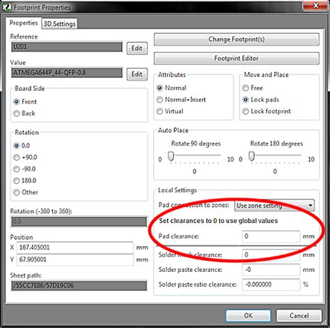
The first step is to create clearance rules specifying the required spacings between objects on different nets. For polyregion-to-pad clearances, this means setting up rules that constrain the relationship between copper pours and pads on different layers.
In a typical rule-driven design environment, clearance rule properties include:
- First and second object types (pads, vias, copper pours, board outlines, etc.)
- Layers or layer pairs the rule applies to
- Minimum and preferred clearance values
- Rule priority relative to other rules
For a polyregion-to-pad rule, copper pours on inner layers would be set as the first object and pads on outer layers as the second object. The specific layers like “Top Layer” and “Ground Layer 2” can be specified. Then the required clearance values, usually taking into account fab capabilities, voltage, and copper weights, are entered.
Running Clearance Checks
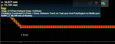
With properly defined rules in place, the PCB design software’s clearance checking features can be used to verify that all spacings between polyregions and pads meet requirements. Clearance checks typically produce graphical and textual design rule check (DRC) reports indicating any violations.
Common issues flagged by polyregion-pad clearance checks include:
- Pad holes covered by polyregion copper
- Polyregion copper too close to pad edges
- Thermal relief connections from pads to polyregion inadequate or missing
Reviewing these reports and adjusting the layout to fix any errors is a crucial step before finalizing the design for manufacturing.
Best Practices for Polyregion-Pad Clearances
Some recommended practices to avoid polyregion-pad clearance issues include:
-
Always refer to the PCB fabrication drawing for required clearances. Never assume or guess.
-
Use conservative spacing values that leave margin. For example, use an 8 mil rule even if the fab can support 6 mil clearances.
-
Pay extra attention to high voltage nets and be sure to follow relevant safety standards.
-
Consider not only clearances but also the potential capacitance between large pads and nearby polyregion fills. Simulate if needed.
-
Define teardrops or thermal reliefs on pads connected to polyregions to facilitate fabrication and assembly while avoiding acid traps.

FAQ
What is the absolute minimum clearance between polyregions and pads?
There is no universal absolute minimum as it depends on the specific PCB fabrication process being used. Always consult with the fab shop and follow their published design rules and guidelines. Generally, most standard commercial PCB processes can support clearances down to 4-6 mils given normal copper weights and layer counts.
Does the shape of the pad affect clearance rules?
Typically no, the clearance rules are based on the minimum gap between any point on the perimeter of the pad and the edge of the polyregion fill. However, unique pad shapes with very acute interior angles may require special consideration to avoid creating acid and etchant traps that are difficult to fabricate.
What if I can’t meet the required clearances due to space constraints?
If the design is tight on space and meeting clearance rules is difficult, there are a few options. First, consider changing the routing and component placement to provide more room. Second, consult with the manufacturer to see if they can support reduced clearances for your design. In some cases, using thinner copper or more precise processes can help. Finally, if clearances simply can’t be met, it may be necessary to enlarge the overall board size.
Are there any IPC standards that deal with polyregion-pad clearances?
While there is no IPC standard that deals with this topic exclusively, the IPC-2221 “Generic Standard on Printed Board Design” does include some general guidance on conductor spacing and clearances. It defines minimum electrical conductor spacings based on voltage levels and also provides general guidelines for spacing based on manufacturing process capabilities. However, always defer to the specific fab drawing from the manufacturer when possible.
What is a typical polyregion-to-pad clearance?
For a standard commercial PCB process using 1 oz copper and carrying moderate voltages under 100V, a typical starting point for polyregion-pad clearance constraints would be around 0.2mm or 8 mils. This provides a good balance between space utilization and manufacturability. However, this may need to be adjusted up or down depending on the specific design requirements and fabrication process being used. Always leave some margin and avoid pushing the absolute minimum clearances unless absolutely necessary.

Conclusion
Maintaining proper clearance between polyregions on inner layers and pads on outer layers is a critical aspect of PCB design. Following design rules and best practices for polyregion-pad clearances helps ensure manufacturability, reliability, and signal integrity. By carefully defining constraints based on fab capabilities, operating voltages, and copper weights, and by running comprehensive clearance checks before signing off on a design, PCB designers can avoid costly respins and field failures. Although it may seem like a minor detail, paying attention to polyregion-pad clearances can make the difference between a successful product and one plagued with problems.

No responses yet