What is a Clamping Circuit?
A clamping circuit, also known as a clamper or DC restorer, is an electronic circuit that fixes either the positive or negative peak of a signal to a defined DC voltage level. Its primary function is to introduce a DC offset to an AC signal, effectively shifting the entire signal up or down to a desired reference voltage.
The clamping circuit is widely used in various electronic applications to prevent signal distortion, maintain proper DC bias, and ensure that the signal remains within a specific voltage range. It is commonly employed in analog signal processing, pulse shaping, and waveform generation.
Components of a Clamping Circuit
A basic clamping circuit consists of three main components:
-
Diode: The diode is the key element in a clamping circuit. It conducts when the input signal exceeds its forward voltage drop, allowing the capacitor to charge or discharge accordingly.
-
Capacitor: The capacitor stores the charge required to maintain the DC offset voltage. Its value determines the time constant of the clamping circuit.
-
Resistor: The resistor provides a path for the capacitor to charge or discharge. It also limits the current flow through the diode.
Types of Clamping Circuits
Clamping circuits can be classified into two main categories based on their clamping action:
1. Positive Clamping Circuit
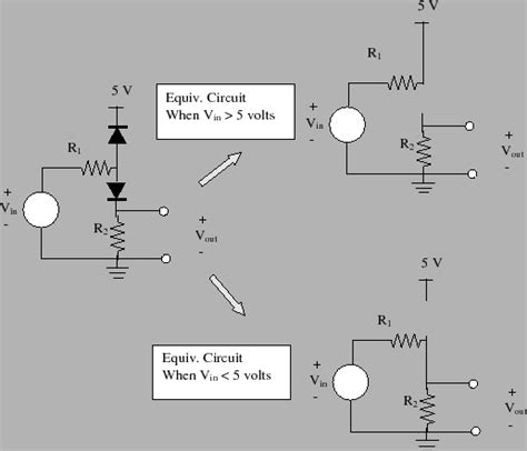
In a positive clamping circuit, the positive peak of the input signal is clamped to a specified DC voltage level. The diode is connected in series with the capacitor, with its cathode connected to the input signal and its anode connected to the reference voltage.
When the input signal exceeds the reference voltage plus the diode’s forward voltage drop, the diode conducts, allowing the capacitor to charge to the peak value of the input signal minus the diode’s forward voltage drop. During the negative half-cycle of the input signal, the diode is reverse-biased, and the capacitor maintains its charge, effectively shifting the entire signal upwards.
2. Negative Clamping Circuit
A negative clamping circuit clamps the negative peak of the input signal to a specified DC voltage level. The diode is connected in series with the capacitor, with its anode connected to the input signal and its cathode connected to the reference voltage.
When the input signal goes below the reference voltage minus the diode’s forward voltage drop, the diode conducts, allowing the capacitor to charge to the negative peak value of the input signal plus the diode’s forward voltage drop. During the positive half-cycle of the input signal, the diode is reverse-biased, and the capacitor maintains its charge, effectively shifting the entire signal downwards.
Clamping Circuit Configurations
Clamping circuits can be configured in various ways to achieve specific clamping actions. Some common configurations include:
-
Biased Clamping Circuit: In a biased clamping circuit, a DC bias voltage is applied to the reference point of the clamping circuit. This allows for clamping the signal to a voltage level other than ground.
-
Dual Clamping Circuit: A dual clamping circuit combines both positive and negative clamping actions to limit the signal within a specific voltage range. It employs two diodes connected in opposite directions, along with two capacitors and resistors.
-
Zener Clamping Circuit: A Zener clamping circuit uses a Zener diode instead of a regular diode to clamp the signal to a precise voltage level determined by the Zener diode’s breakdown voltage.

Applications of Clamping Circuits
Clamping circuits find applications in various domains of electronics and electrical engineering. Some notable applications include:
- Analog Signal Processing:
- Clamping circuits are used to restore the DC component of an AC-coupled signal, ensuring proper biasing and preventing signal distortion.
-
They are employed in video signal processing to maintain the black level reference and prevent picture distortion.
-
Waveform Generation:
- Clamping circuits are used to generate specific waveforms by clamping a portion of the input signal to a desired voltage level.
-
They are utilized in pulse shaping circuits to generate square waves, sawtooth waves, and other custom waveforms.
-
Voltage Level Shifting:
- Clamping circuits are employed to shift the voltage level of a signal to match the input requirements of subsequent stages in a circuit.
-
They are used in interfacing circuits to convert between different voltage levels, such as TTL to CMOS or vice versa.
-
Overvoltage Protection:
- Clamping circuits can be used to protect sensitive electronic components from overvoltage conditions by clamping the voltage to a safe level.
-
They are employed in power supply circuits and voltage regulators to limit the output voltage within a specified range.
-
Noise Reduction:
- Clamping circuits can help in reducing noise and interference in electronic systems by clamping the signal to a stable reference voltage.
- They are used in audio and communication systems to minimize the impact of noise and ensure signal integrity.

Designing a Clamping Circuit
When designing a clamping circuit, several factors need to be considered to ensure optimal performance:
- Diode Selection:
- Choose a diode with a suitable forward voltage drop and current rating based on the input signal characteristics and the desired clamping voltage.
-
Schottky diodes are commonly used in clamping circuits due to their low forward voltage drop and fast switching speeds.
-
Capacitor Value:
- The capacitor value determines the time constant of the clamping circuit, which affects the response time and the ability to track the input signal.
-
A larger capacitor value results in a slower response but better tracking of the input signal, while a smaller value provides faster response but may introduce distortion.
-
Resistor Value:
- The resistor value influences the charging and discharging time of the capacitor and the overall impedance of the clamping circuit.
-
A higher resistor value slows down the charging and discharging process, while a lower value allows for faster response but may load the input signal source.
-
Reference Voltage:
- Choose an appropriate reference voltage based on the desired clamping level and the input signal range.
-
Consider the voltage drop across the diode and the maximum voltage rating of the components when selecting the reference voltage.
-
Signal Frequency:
- The clamping circuit’s performance is affected by the frequency of the input signal.
- Ensure that the clamping circuit’s time constant is appropriately chosen to accommodate the signal frequency range of interest.
Clamping Circuit Design Example
Let’s consider an example of designing a positive clamping circuit to clamp a sinusoidal input signal with a peak-to-peak voltage of 10V to a DC level of 5V.
Given:
– Input signal: Sinusoidal, 10V peak-to-peak
– Desired clamping voltage: 5V DC
Step 1: Select the diode
– Choose a Schottky diode with a forward voltage drop of 0.3V and a suitable current rating.
Step 2: Determine the capacitor value
– The capacitor value should be chosen based on the input signal frequency and the desired response time.
– For this example, let’s assume a capacitor value of 1μF.
Step 3: Calculate the resistor value
– The resistor value should be selected to provide an appropriate charging and discharging time constant.
– A resistor value of 10kΩ can be chosen for this example.
Step 4: Verify the clamping voltage
– The clamping voltage will be approximately 5V minus the diode’s forward voltage drop.
– Clamping voltage = 5V – 0.3V = 4.7V
The designed clamping circuit will clamp the positive peak of the 10V peak-to-peak sinusoidal input signal to approximately 4.7V DC.

Clamping Circuit Analysis
To analyze the behavior of a clamping circuit, we need to consider the circuit’s operation during different stages of the input signal.
Positive Clamping Circuit Analysis
Consider a positive clamping circuit with the following components:
– Input signal: Sinusoidal, amplitude Vm, frequency f
– Diode: Forward voltage drop VD
– Capacitor: Capacitance C
– Resistor: Resistance R
– Reference voltage: Vref
During the positive half-cycle of the input signal:
– When the input voltage exceeds Vref + VD, the diode conducts, and the capacitor charges to the peak value of the input signal minus the diode’s forward voltage drop.
– Capacitor voltage VC = Vm – VD
During the negative half-cycle of the input signal:
– The diode is reverse-biased, and the capacitor maintains its charge.
– The output voltage Vout is the sum of the input voltage and the capacitor voltage.
– Vout = Vin + VC
The time constant τ of the clamping circuit is given by:
– τ = RC
The time constant determines the charging and discharging time of the capacitor and affects the clamping circuit’s response to changes in the input signal.
Negative Clamping Circuit Analysis
The analysis of a negative clamping circuit follows a similar approach, with the diode connected in the opposite direction and the capacitor charging to the negative peak value of the input signal plus the diode’s forward voltage drop.
Clamping Circuit Limitations and Considerations
While clamping circuits are useful in various applications, they have certain limitations and considerations that need to be addressed:
- Diode Non-Idealities:
- Real diodes have a finite forward voltage drop and reverse leakage current, which can affect the accuracy of the clamping voltage.
-
The diode’s non-ideal characteristics can introduce distortion and affect the circuit’s performance, especially at high frequencies.
-
Capacitor Leakage:
- Practical capacitors have leakage current, which can cause the clamping voltage to drift over time.
-
Leakage current becomes more significant in high-impedance circuits and can impact the long-term stability of the clamping voltage.
-
Signal Distortion:
- Clamping circuits can introduce distortion to the input signal, particularly during the charging and discharging of the capacitor.
-
The amount of distortion depends on factors such as the signal frequency, capacitor value, and diode characteristics.
-
Frequency Limitations:
- The clamping circuit’s performance is frequency-dependent due to the time constant of the RC network.
-
At high frequencies, the clamping action may not be effective, leading to incomplete clamping or signal distortion.
-
Loading Effect:
- The clamping circuit presents a load to the input signal source, which can affect the signal’s amplitude and shape.
-
The loading effect becomes more significant when using low-value resistors or when the input signal source has a high output impedance.
-
Bias Current:
- The clamping circuit requires a small bias current to maintain the clamping voltage across the capacitor.
- The bias current can introduce a small DC offset in the output signal, which may need to be considered in certain applications.
Frequently Asked Questions (FAQ)
-
What is the purpose of a clamping circuit?
A clamping circuit is used to introduce a DC offset to an AC signal, effectively shifting the entire signal up or down to a desired reference voltage. It helps in maintaining proper DC biasing, preventing signal distortion, and ensuring that the signal remains within a specific voltage range. -
What are the main components of a clamping circuit?
The main components of a clamping circuit are a diode, a capacitor, and a resistor. The diode conducts when the input signal exceeds a certain threshold, allowing the capacitor to charge or discharge. The resistor provides a path for the capacitor to charge or discharge and limits the current flow through the diode. -
What is the difference between a positive and negative clamping circuit?
A positive clamping circuit clamps the positive peak of the input signal to a specified DC voltage level, shifting the entire signal upwards. On the other hand, a negative clamping circuit clamps the negative peak of the input signal to a specified DC voltage level, shifting the entire signal downwards. -
How does the capacitor value affect the clamping circuit’s performance?
The capacitor value determines the time constant of the clamping circuit, which affects the response time and the ability to track the input signal. A larger capacitor value results in a slower response but better tracking of the input signal, while a smaller value provides faster response but may introduce distortion. -
What are some common applications of clamping circuits?
Clamping circuits find applications in various areas, including analog signal processing, waveform generation, voltage level shifting, overvoltage protection, and noise reduction. They are used in video signal processing, pulse shaping circuits, interfacing circuits, power supply circuits, and audio and communication systems.
Conclusion
Clamping circuits play a crucial role in electronic systems by introducing a DC offset to AC signals, maintaining proper biasing, and preventing signal distortion. They find widespread use in analog signal processing, waveform generation, voltage level shifting, overvoltage protection, and noise reduction applications.
Understanding the types of clamping circuits, their configurations, and design considerations is essential for effectively implementing them in electronic circuits. By selecting appropriate components, such as diodes, capacitors, and resistors, and considering factors like signal frequency and desired clamping voltage, designers can optimize the performance of clamping circuits.
While clamping circuits offer numerous benefits, it is important to be aware of their limitations and considerations, such as diode non-idealities, capacitor leakage, signal distortion, frequency limitations, loading effects, and bias current. Addressing these factors ensures the reliable and efficient operation of clamping circuits in various applications.
As technology advances and new electronic systems emerge, the significance of clamping circuits continues to grow. Their versatility and ability to manipulate and condition signals make them indispensable in modern electronic design. By leveraging the principles and techniques discussed in this article, engineers and designers can effectively harness the power of clamping circuits to enhance the performance and reliability of their electronic systems.
No responses yet