Introduction to Ceramic PCB
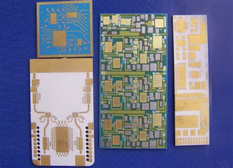
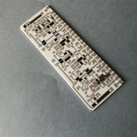
Ceramic Printed Circuit Boards (PCBs) have gained significant popularity in recent years due to their unique properties and advantages over traditional PCBs. These boards are made from ceramic materials, such as alumina or aluminum nitride, which offer excellent thermal conductivity, high dielectric strength, and low dielectric loss. Ceramic PCBs are widely used in various industries, including aerospace, automotive, medical, and telecommunications, where high reliability and performance are critical.
In this comprehensive guide, we will dive deep into the world of Ceramic PCBs, exploring their benefits, applications, manufacturing processes, and customization options. By the end of this article, you will have a thorough understanding of how Ceramic PCBs can revolutionize your electronic projects in 2023 and beyond.
Advantages of Ceramic PCB
1. Excellent Thermal Conductivity
One of the most significant advantages of Ceramic PCBs is their excellent thermal conductivity. Ceramic materials, such as alumina, have a thermal conductivity of up to 30 W/mK, which is significantly higher than that of traditional FR-4 PCBs (0.3 W/mK). This property allows Ceramic PCBs to efficiently dissipate heat generated by electronic components, preventing thermal damage and ensuring optimal performance.
2. High Dielectric Strength
Ceramic PCBs have a high dielectric strength, which is the maximum electric field strength that a material can withstand without breaking down. This property enables Ceramic PCBs to operate at higher voltages without the risk of dielectric breakdown, making them suitable for high-power applications.
3. Low Dielectric Loss
Ceramic materials have a low dielectric loss, which means they have minimal energy dissipation when subjected to an alternating electric field. This property is essential for high-frequency applications, as it reduces signal loss and improves signal integrity.
4. Dimensional Stability
Ceramic PCBs have excellent dimensional stability, meaning they maintain their shape and size under various environmental conditions, such as temperature fluctuations and humidity. This stability is crucial for applications that require precise component placement and alignment.
5. Chemical and Corrosion Resistance
Ceramic materials are highly resistant to chemicals and corrosion, making Ceramic PCBs suitable for harsh environments. They can withstand exposure to acids, bases, and other corrosive substances without degradation, ensuring long-term reliability.
Applications of Ceramic PCB
1. Aerospace and Defense
Ceramic PCBs are widely used in the aerospace and defense industries due to their ability to withstand extreme temperatures, vibrations, and shock. They are used in satellites, missiles, and other high-performance systems where reliability is paramount.
2. Automotive
The automotive industry has embraced Ceramic PCBs for their excellent thermal management capabilities and resistance to harsh environments. They are used in engine control units, power modules, and other critical electronic systems.
3. Medical Devices
Ceramic PCBs are used in various medical devices, such as implantable devices and diagnostic equipment, due to their biocompatibility and high reliability. They can withstand sterilization processes and operate in close proximity to the human body without causing harm.
4. Telecommunications
In the telecommunications industry, Ceramic PCBs are used in high-frequency applications, such as 5G networks and satellite communication systems. Their low dielectric loss and high signal integrity make them ideal for these applications.
5. Power Electronics
Ceramic PCBs are used in power electronic systems, such as inverters, converters, and motor drives, due to their high dielectric strength and excellent thermal management. They can handle high voltages and currents while maintaining optimal performance.

Manufacturing Process of Ceramic PCB
The manufacturing process of Ceramic PCBs differs from that of traditional PCBs due to the unique properties of ceramic materials. Here’s a step-by-step overview of the process:
-
Substrate Preparation: The ceramic substrate, typically alumina or aluminum nitride, is cut to the desired size and shape.
-
Via Drilling: Holes are drilled into the ceramic substrate to create vias, which are used to connect different layers of the PCB.
-
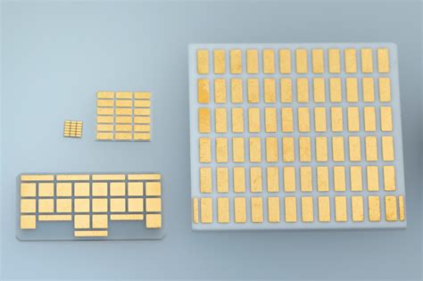
Metallization: A thin layer of metal, such as copper or gold, is deposited onto the ceramic substrate using techniques like sputtering or electroplating.
-
Patterning: The desired circuit pattern is created on the metallized substrate using photolithography or screen printing.
-
Etching: The unwanted metal areas are removed using a chemical etching process, leaving only the desired circuit pattern.
-
Lamination: If a multi-layer Ceramic PCB is required, additional ceramic layers are stacked and laminated together using high pressure and temperature.
-
Singulation: The laminated board is cut into individual PCBs using a dicing saw or laser cutting.
-
Surface Finishing: The exposed metal surfaces are coated with a protective layer, such as nickel/gold or silver, to prevent oxidation and improve solderability.
-
Inspection and Testing: The finished Ceramic PCBs undergo rigorous inspection and testing to ensure they meet the required specifications and performance criteria.
Customization Options for Ceramic PCB
One of the key advantages of Ceramic PCBs is their high degree of customization. Here are some of the customization options available:
1. Substrate Material
Alumina and aluminum nitride are the most common ceramic substrate materials, but other options, such as beryllia and silicon nitride, are also available. Each material has its own unique properties, and the choice depends on the specific application requirements.
2. Layer Count
Ceramic PCBs can be manufactured with a single layer or multiple layers, depending on the complexity of the circuit design. Multi-layer Ceramic PCBs offer higher circuit density and better signal integrity.
3. Via Type
There are several types of vias available for Ceramic PCBs, including through-hole vias, blind vias, and buried vias. The choice of via type depends on the circuit design and the required level of interconnectivity.
4. Metallization
Copper and gold are the most common metallization options for Ceramic PCBs, but other metals, such as silver and palladium, can also be used. The choice of metal depends on the desired electrical and thermal properties, as well as the compatibility with the substrate material.
5. Surface Finish
Various surface finishes are available for Ceramic PCBs, including nickel/gold, silver, and tin. The choice of surface finish depends on the solderability requirements, environmental conditions, and the desired aesthetics.
6. Embedded Components
Ceramic PCBs can accommodate embedded components, such as resistors and capacitors, within the substrate layers. This feature allows for higher component density and improved signal integrity.
Choosing the Right Ceramic PCB Manufacturer
Selecting the right Ceramic PCB manufacturer is crucial to ensure the success of your electronic project. Here are some factors to consider when choosing a manufacturer:
-
Experience and Expertise: Look for a manufacturer with extensive experience in producing Ceramic PCBs and a deep understanding of the unique challenges associated with ceramic materials.
-
Quality Control: Ensure that the manufacturer has a robust quality control system in place, including strict process controls, inspections, and testing procedures.
-
Certifications: Choose a manufacturer with relevant certifications, such as ISO 9001, ISO 14001, and IATF 16949, to ensure they adhere to industry standards and best practices.
-
Customization Capabilities: Verify that the manufacturer can accommodate your specific customization requirements, such as substrate material, layer count, via type, and surface finish.
-
Lead Time and Pricing: Consider the manufacturer’s lead time and pricing structure to ensure they align with your project timeline and budget.
-
Customer Support: Look for a manufacturer that offers excellent customer support, including responsive communication, technical assistance, and after-sales service.
Frequently Asked Questions (FAQ)
1. What is the difference between Ceramic PCBs and traditional PCBs?
Ceramic PCBs are made from ceramic materials, such as alumina or aluminum nitride, while traditional PCBs are made from organic materials, such as FR-4. Ceramic PCBs offer superior thermal conductivity, high dielectric strength, low dielectric loss, and excellent dimensional stability compared to traditional PCBs.
2. Are Ceramic PCBs more expensive than traditional PCBs?
Yes, Ceramic PCBs are generally more expensive than traditional PCBs due to the higher cost of ceramic materials and the specialized manufacturing processes involved. However, the superior performance and reliability of Ceramic PCBs often justify the additional cost for critical applications.
3. Can Ceramic PCBs be used for high-frequency applications?
Yes, Ceramic PCBs are well-suited for high-frequency applications due to their low dielectric loss and high signal integrity. They are commonly used in telecommunications, aerospace, and defense industries for applications such as 5G networks, satellite communication, and radar systems.
4. How do Ceramic PCBs handle thermal management?
Ceramic PCBs have excellent thermal conductivity, which allows them to efficiently dissipate heat generated by electronic components. This property helps prevent thermal damage and ensures optimal performance, even in high-power applications.
5. Are Ceramic PCBs suitable for harsh environments?
Yes, Ceramic PCBs are highly resistant to chemicals, corrosion, and extreme temperatures, making them suitable for harsh environments. They can withstand exposure to acids, bases, and other corrosive substances without degradation, ensuring long-term reliability in challenging conditions.
Conclusion
Ceramic PCBs offer a wide range of benefits and customization options for electronic projects that require high performance, reliability, and durability. Their excellent thermal conductivity, high dielectric strength, low dielectric loss, and dimensional stability make them ideal for applications in aerospace, automotive, medical, telecommunications, and power electronics industries.
By understanding the advantages, manufacturing processes, and customization options of Ceramic PCBs, you can make informed decisions when designing and implementing your electronic projects. Choosing the right Ceramic PCB manufacturer is also crucial to ensure the success of your project, considering factors such as experience, quality control, certifications, customization capabilities, lead time, pricing, and customer support.
As technology continues to advance, Ceramic PCBs will play an increasingly important role in enabling the development of cutting-edge electronic systems. By staying up-to-date with the latest trends and best practices in Ceramic PCB Design and manufacturing, you can unlock new possibilities and take your electronic projects to the next level in 2023 and beyond.
Comparison Table: Ceramic PCBs vs. Traditional PCBs
| Property | Ceramic PCBs | Traditional PCBs |
|---|---|---|
| Thermal Conductivity | High | Low |
| Dielectric Strength | High | Moderate |
| Dielectric Loss | Low | Moderate |
| Dimensional Stability | Excellent | Good |
| Chemical Resistance | High | Moderate |
| Corrosion Resistance | High | Moderate |
| Suitable for High-Power | Yes | Limited |
| Suitable for High-Freq. | Yes | Limited |
| Cost | High | Low to Moderate |
This table provides a quick comparison of the key properties of Ceramic PCBs and traditional PCBs, highlighting the superior performance of Ceramic PCBs in terms of thermal conductivity, dielectric strength, dielectric loss, dimensional stability, chemical resistance, and corrosion resistance. While Ceramic PCBs are more expensive than traditional PCBs, their advanced properties make them suitable for high-power and high-frequency applications.
No responses yet