Introduction to the CD4013 Dual D Flip-Flop Chip
The CD4013 is a CMOS dual D-type flip-flop integrated circuit. It is part of the 4000 series of CMOS logic chips originally introduced by RCA in the 1970s. The CD4013 contains two independent D-type flip-flops with set and reset capability. This versatile chip is used in a wide variety of digital circuits and electronic projects.
Key Features of the CD4013
- Dual D-type flip-flops in a single package
- Set and reset inputs for each flip-flop
- Q and Q̄ (not Q) outputs for each flip-flop
- Wide supply voltage range: 3V to 15V
- Low power consumption
- High noise immunity
- Suitable for low-frequency applications
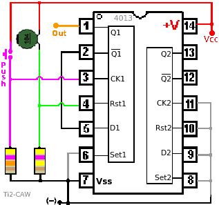
CD4013 Pinout and Pin Functions
The CD4013 is available in several package types, including PDIP (Plastic Dual In-line Package), SOIC (Small Outline Integrated Circuit), and TSSOP (Thin Shrink Small Outline Package). The most common package is the 14-pin PDIP.
CD4013 Pinout Diagram
| Pin Number | Pin Name | Description |
|---|---|---|
| 1 | Q1 | Output of flip-flop 1 |
| 2 | Q̄1 | Inverted output of flip-flop 1 |
| 3 | CLK1 | Clock input for flip-flop 1 |
| 4 | RST1 | Reset input for flip-flop 1 |
| 5 | D1 | Data input for flip-flop 1 |
| 6 | SET1 | Set input for flip-flop 1 |
| 7 | VSS | Ground (0V) |
| 8 | SET2 | Set input for flip-flop 2 |
| 9 | D2 | Data input for flip-flop 2 |
| 10 | RST2 | Reset input for flip-flop 2 |
| 11 | CLK2 | Clock input for flip-flop 2 |
| 12 | Q̄2 | Inverted output of flip-flop 2 |
| 13 | Q2 | Output of flip-flop 2 |
| 14 | VDD | Positive supply voltage (3V to 15V) |
Pin Functions
-
Q and Q̄: These are the non-inverted and inverted outputs of the flip-flop, respectively. When the flip-flop is triggered, the Q output takes the state of the D input, while Q̄ takes the opposite state.
-
CLK: The clock input triggers the flip-flop on its rising edge. When the clock transitions from low to high, the state of the D input is transferred to the Q output.
-
RST: The reset input is active low. When RST is held low, the flip-flop is reset, setting Q to low and Q̄ to high, regardless of the states of the other inputs.
-
D: This is the data input of the flip-flop. The state of D is transferred to Q on the rising edge of the clock signal, provided that SET and RST are both high.
-
SET: The set input is active low. When SET is held low, the flip-flop is set, forcing Q to high and Q̄ to low, regardless of the states of the other inputs.
-
VSS and VDD: These pins are used for the power supply. VSS is connected to ground (0V), while VDD is connected to the positive supply voltage, which can range from 3V to 15V.

CD4013 Operation and Timing Diagram
The CD4013 is a positive-edge-triggered D-type flip-flop. This means that the state of the D input is transferred to the Q output on the rising edge of the clock signal, provided that the SET and RST inputs are both high.
When the SET input is low, the flip-flop is forced into the set state, with Q high and Q̄ low, regardless of the states of the other inputs. Similarly, when the RST input is low, the flip-flop is forced into the reset state, with Q low and Q̄ high.
Timing Diagram
      ___________          ___________
CLK  /           \________/           \_______
     ___________                  ___________
D   /           \________________/
     ___________                  ___________
Q                ________________/
     ___________                  ___________
Q̄   \           ________________/
     ___________                  ___________
SET  \           /
     ___________                  ___________
RST              \______________/
In this timing diagram:
1. When the clock (CLK) transitions from low to high, the state of D is transferred to Q, and Q̄ takes the opposite state.
2. When SET goes low, Q is forced high, and Q̄ is forced low, regardless of the states of the other inputs.
3. When RST goes low, Q is forced low, and Q̄ is forced high, regardless of the states of the other inputs.

CD4013 Application Circuits
The CD4013 can be used in a variety of digital circuits, such as flip-flop-based counters, shift registers, frequency dividers, and data synchronizers. Here are a few example application circuits:
Frequency Divider
A frequency divider is a circuit that takes an input clock signal and produces an output signal with a frequency that is a fraction of the input frequency. The CD4013 can be used to create a simple divide-by-2 frequency divider.
        VDD
         |
        .-.
        | |
        | | R1
        | | 10k
        '-'
         |
        .-.
        | |
        | | R2
        | | 10k
        '-'
         |
        .-. D1     Q1 .--------.
CLK ----|>|---+----|C| CD4013 |
        '-'   |    '-|        |
              '--+---|R       |
                 |   '--------'
                 |
                 |
                .-.
                |<|-Q̄1
                '-'
                 |
                ===
                GND
In this circuit:
1. The Q̄1 output is connected to the D1 input, creating a feedback loop.
2. On each rising edge of the input clock signal, the state of Q̄1 is transferred to Q1, and Q̄1 takes the opposite state.
3. The result is an output signal at Q1 with a frequency that is half of the input clock frequency.
Debounce Circuit
Mechanical switches and buttons can produce multiple transitions when pressed or released, causing unwanted multiple pulses in digital circuits. A debounce circuit is used to eliminate these unwanted transitions and provide a clean, single pulse output. The CD4013 can be used as part of a simple debounce circuit.
        VDD
         |
        .-.
        | |
        | | R1
        | | 10k
        '-'
         |
        .-.  Q̄1     Q1 .--------.
SW1 ----|>|---+----|C| CD4013 |
        '-'   |    '-|        |
              '--+---|R       |
                 |   '--------'
                 |
                 | R2
                 | 10k
                 |
                 |
                .-.
                |<|-D1
                '-'
                 |
                ===
                GND
In this debounce circuit:
1. When the switch (SW1) is pressed, the D1 input is pulled high through resistor R1.
2. The high state of D1 is transferred to Q1 on the next rising edge of the clock signal, which is generated by the switch itself.
3. The Q1 output remains high until the switch is released, at which point D1 is pulled low through resistor R2.
4. The low state of D1 is transferred to Q1 on the next rising edge of the clock signal, causing Q1 to go low.
5. The result is a clean, debounced output signal at Q1 that reflects the state of the switch.

CD4013 Datasheet and Specifications
For detailed information on the CD4013, including electrical characteristics, timing specifications, and package dimensions, refer to the manufacturer’s datasheet. Some key specifications are:
- Supply Voltage Range: 3V to 15V
- Input Voltage Range: 0V to VDD
- Output Voltage Range: 0V to VDD
- Propagation Delay: 140ns (typical) at VDD = 10V
- Power Dissipation: 50μW (typical) at VDD = 10V
- Operating Temperature Range: -55°C to 125°C
Always consult the datasheet provided by the manufacturer of the specific CD4013 variant you are using to ensure proper operation and design considerations.
Frequently Asked Questions (FAQ)
1. What is the difference between the CD4013 and the 74HC74?
The CD4013 is a CMOS dual D-type flip-flop, while the 74HC74 is a high-speed CMOS dual D-type flip-flop. The main differences are:
- The CD4013 is part of the 4000 series of CMOS logic, while the 74HC74 is part of the 74HC series.
- The CD4013 has a wider supply voltage range (3V to 15V) compared to the 74HC74 (2V to 6V).
- The 74HC74 has faster switching speeds and lower propagation delays than the CD4013.
2. Can the CD4013 be used as a latch?
Yes, the CD4013 can be used as a latch by connecting the SET and RST inputs to the appropriate logic levels. When SET is low, the flip-flop is forced into the set state (Q high, Q̄ low), and when RST is low, the flip-flop is forced into the reset state (Q low, Q̄ high), regardless of the clock signal.
3. How do I choose the appropriate resistor values for a CD4013 circuit?
The resistor values in a CD4013 circuit depend on factors such as the supply voltage, the desired current consumption, and the switching speed requirements. In general, pull-up resistors in the range of 1kΩ to 10kΩ are common for input pins, while output pins may require lower values to drive higher loads. Always consider the specific requirements of your application and consult the CD4013 datasheet for guidance.
4. Can I use the CD4013 in a 5V logic system?
Yes, the CD4013 is compatible with 5V logic systems, as its supply voltage range includes 5V. However, keep in mind that the input and output voltage levels will be different compared to other 5V logic families like TTL. The CD4013 inputs will recognize a high state at around 3.5V (70% of VDD), while TTL inputs typically require a higher voltage for a high state.
5. What are some common applications for the CD4013?
The CD4013 is widely used in various digital circuits and applications, such as:
- Frequency dividers
- Debounce circuits for switches and buttons
- Shift registers
- Counters
- Data synchronizers
- Pulse Generators
- Memory elements in digital systems
Its versatility, wide supply voltage range, and low power consumption make the CD4013 a popular choice for many electronic projects and designs.
Conclusion
The CD4013 dual D-type flip-flop is a versatile and widely used CMOS logic chip that finds applications in numerous digital circuits. With its set and reset capabilities, wide supply voltage range, and low power consumption, the CD4013 is an essential component in many electronic projects.
By understanding the CD4013’s pinout, operation, and application circuits, you can effectively utilize this chip in your designs. Always refer to the manufacturer’s datasheet for detailed specifications and guidelines to ensure proper integration and functionality.
No responses yet