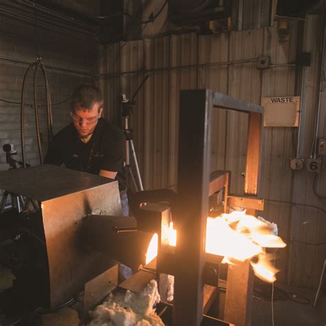
what burn testing electronics
Introduction to Burn Testing Burn-testing, also known as burn-in testing, is a critical process in the electronics industry that involves subjecting electronic components, devices, or[…]
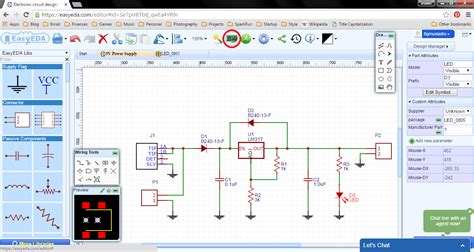
What s New in Eagle V6 PCB Design Software
Enhanced User Interface and Customization One of the first things you’ll notice in Eagle V6 is the sleek new user interface. The streamlined UI puts[…]
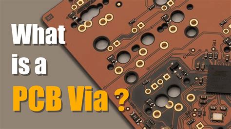
Tenting Via – The Ultimate Guide To The Importance of PCBs
What is PCB Tenting? PCB tenting refers to the process of covering drilled holes (vias) in a printed circuit board with solder mask material. Tenting[…]
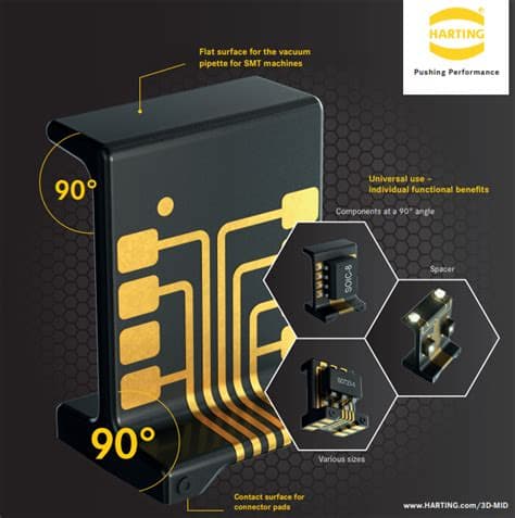
What Are Molded Interconnect Devices or MIDs?
What are Molded Interconnect Devices? Molded Interconnect Devices, or MIDs, are three-dimensional (3D) injection-molded plastic parts with integrated electronic circuits. These devices combine the mechanical[…]
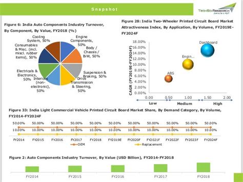
automotive pcb market shares pcb designers market growth
Introduction to the automotive PCB market The automotive industry has undergone a significant transformation in recent years, with the increasing adoption of advanced electronics and[…]

weekly digest john coonrad pcb industry experts
Introduction to John Coonrad and His PCB Industry Insights John Coonrad is a leading expert in the printed circuit board (PCB) industry, with over 30[…]
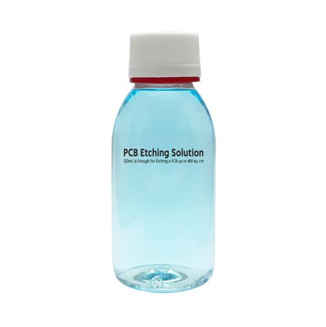
wet and dry pcb etching solutions which process right solution
What is PCB Etching? PCB etching is the process of removing unwanted copper from a PCB using a chemical or physical process. The goal is[…]
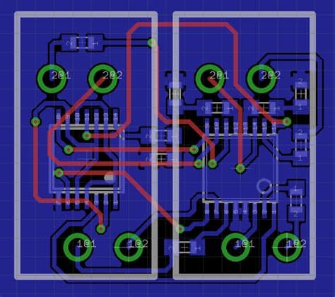
Everything You Need to Know about Designing a PCB Layout
Introduction to PCB Layout Design Printed Circuit Board (PCB) layout design is a crucial step in the development of electronic devices. It involves the arrangement[…]
PCB Color – How To Select The Color You Need
Why Does PCB Color Matter? The color of a PCB is not just a cosmetic choice; it can have a direct impact on the board’s[…]
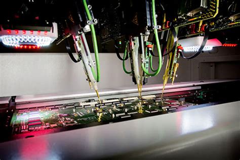
The Ultimate Guide to Flying Probe Test in PCBA
What is Flying Probe Test? Flying probe test is an advanced method used in the printed circuit board assembly (PCBA) process to test the functionality[…]