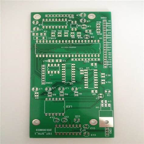
design reuse methodologies and best practices for re applying previous boards
Introduction to Design Reuse Design reuse is a crucial strategy in PCB design that involves leveraging existing designs, components, and intellectual property (IP) to create[…]
start your schematic right best electronics parts management
Introduction to Schematic Parts Management As an electronics enthusiast or professional, you know that creating a well-organized and efficient schematic is crucial for the success[…]
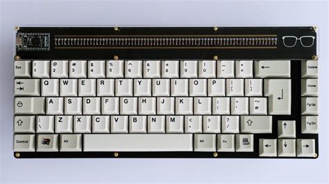
How to make a construction process of open source ergonomic Keyboard PCB project
Introduction to Open Source Keyboard PCB Projects Open source keyboard PCB projects have gained popularity among DIY enthusiasts and keyboard enthusiasts alike. These projects allow[…]
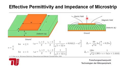
Stripline vs. Microstrip: A Comparison Between High-Frequency Signal Transmission Lines
Introduction to Stripline and Microstrip In the world of high-frequency electronics, the choice of signal transmission lines plays a crucial role in ensuring the integrity[…]
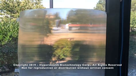
stealth aircraft meet quantum radar
Introduction to Stealth Technology and Quantum Radar Stealth technology has been a game-changer in modern warfare, allowing aircraft to evade detection by traditional radar systems.[…]

steaming hot steampunk news
The Rise of Steampunk Fashion One of the most visible aspects of steampunk culture is its distinctive fashion style. Steampunk fashion often features elements such[…]
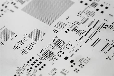
What is stencil for pcb
Introduction to PCB Stencils Printed Circuit Board (PCB) stencils are essential tools in the electronics manufacturing industry. They are thin, flat sheets of metal or[…]
What is PCB stencil
Why Use a PCB Stencil? PCB stencils are essential for several reasons: Precision: Stencils ensure that the correct amount of solder paste is applied to[…]
sub 25 micron traces averatek asap technology
Introduction to Averatek ASAP Averatek ASAP (Advanced Subtractive Additive Process) is a groundbreaking technology that enables the creation of high-density printed circuit boards (PCBs) with[…]
stubs transmission lines what do they do and how do you keep them happening
Introduction to Stub Transmission Lines Stub transmission lines are a crucial component in the world of electrical engineering and telecommunications. These specialized transmission lines play[…]