Copper fills – mechanically speaking
Introduction to Copper fills Copper fills, also known as copper fill-ins or copper filling, is a technique used in printed circuit board (PCB) manufacturing to[…]
Let’s talk about PCB Outlines
What are Best Practices for Designing PCB Outlines To ensure successful PCB Design and manufacturing, follow these best practices when defining PCB outlines: Start with[…]
KiCAD – Rayming reads in native KiCAD-data
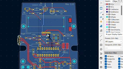
Introduction to KiCAD and Rayming KiCAD is a popular open-source Electronic Design automation (EDA) software that allows users to design printed circuit boards (PCBs) from[…]

The Rapid Evolution of Electronic Manufacturing Services for Medtech
Introduction to Medtech EMS The medical technology (medtech) industry has seen remarkable growth and innovation in recent years. As medical devices become more complex and[…]
The Leading Medical PCB Manufacturer for Assembly
What Makes Medical PCBs Different? Medical PCBs are designed and manufactured specifically for use in medical devices and equipment. These PCBs must meet stringent quality[…]

EAGLE and DesignLink – Valuable information about components
What is EAGLE? EAGLE (Easily Applicable Graphical Layout Editor) is a powerful PCB (Printed Circuit Board) design software developed by Autodesk. It is widely used[…]
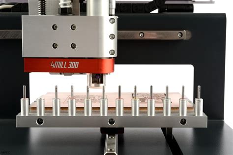
Indicating slots, milling, contour and rout-outs in your PCB design.
Introduction to PCB Machining Printed Circuit Board (PCB) machining is an essential process in the manufacturing of electronic devices. It involves creating holes, slots, and[…]
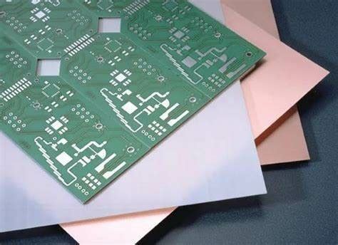
PCB services based on material choice
Introduction to PCB Material Selection Printed Circuit Boards (PCBs) are the backbone of modern electronics, providing a platform for components to be mounted and interconnected.[…]
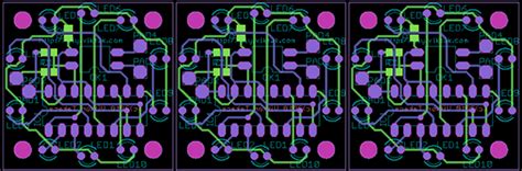
How to Panelise Small PCBs
What is PCB Panelisation? PCB panelisation is the process of combining multiple small printed circuit boards (PCBs) onto a single large panel for manufacturing. This[…]
Phototools for PCB image transfer
What are Phototools in PCB Manufacturing? Phototools are high-resolution, transparent films that carry the circuit pattern for a PCB. They are used in the photolithography[…]