rf power supply design and layout guide
Introduction Radio Frequency (RF) power supplies are essential components in various applications, including telecommunications, broadcasting, and industrial processes. Designing and laying out an efficient and[…]
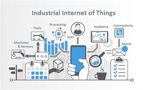
rf signal chain and link budget basics iot
Introduction to RF-IoT-Basics The Internet of Things (IoT) has revolutionized the way we interact with devices and collect data from our surroundings. At the heart[…]
dont get caught sleeping resolve pcb power distribution problems
Understanding PCB Power Distribution Proper PCB power distribution is critical for ensuring your electronic devices function reliably without issues like excessive heat generation, electromagnetic interference,[…]
rick hartley on 6 layer boards and power delivery 3
Introduction to 6 Layer PCBs and Power Delivery Six-layer printed circuit boards (PCBs) have become increasingly popular in the electronics industry due to their ability[…]
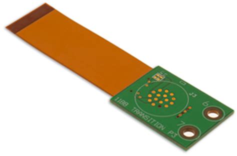
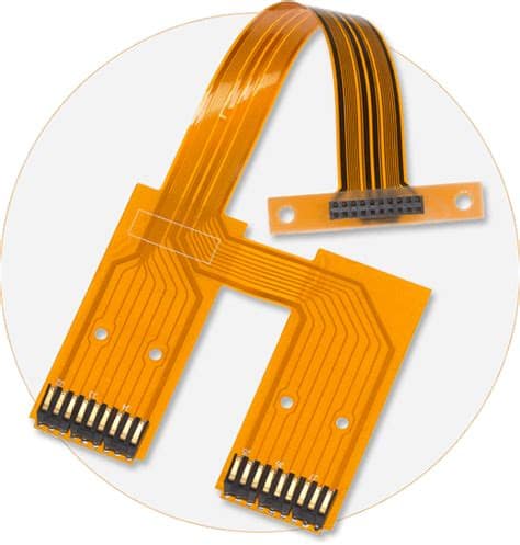
rigid flex cost comparison
Introduction to Rigid-Flex PCBs Rigid-flex PCBs are a unique combination of rigid and flexible printed circuit boards that offer numerous advantages over traditional PCBs. They[…]

Role Isu Petasys Multilayer Manufacturing Company Realizing Successful Pcb Implementation
Introduction to ISU Petasys ISU Petasys is a leading multilayer manufacturing company that specializes in the production of high-quality printed circuit boards (PCBs). With their[…]
Routing Topologies In Your Pcb And Computer Peripherals
Introduction to Routing Topologies Routing topologies play a crucial role in the design and functionality of printed circuit boards (PCBs) and computer peripherals. These topologies[…]
cad software for pcb design
What is PCB CAD Software? PCB CAD (computer-aided design) software is specialized electronic design automation (EDA) tools used to design printed circuit boards (PCBs). PCB[…]
rule tips pcb height restrictions
Understanding PCB Height and Its Importance Printed Circuit Board (PCB) height is a crucial factor to consider when designing and manufacturing electronic devices. The height[…]
sap and msap in flexible circuit fabrication
Introduction to Flexible Circuits and SAP/mSAP Flexible circuits, also known as flex circuits or flexible printed circuit boards (PCBs), are a type of electronic circuit[…]