
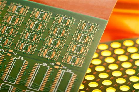
promising and challenging future 3d printed electronics
What are 3D-Printed Electronics? 3D-printed electronics refer to electronic devices and components that are fabricated using additive manufacturing techniques. Unlike traditional electronics manufacturing, which involves[…]
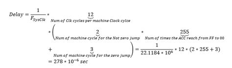
propagation delay calculator
Understanding Propagation Delay Propagation delay is a critical concept in the world of electronics and digital communication. It refers to the time taken for a[…]

propagation delay transmission delay and analog signal resonance your pcb
Introduction to Signal Delay on Printed Circuit Boards Signal delay is a critical factor to consider when designing and manufacturing printed circuit boards (PCBs). It[…]
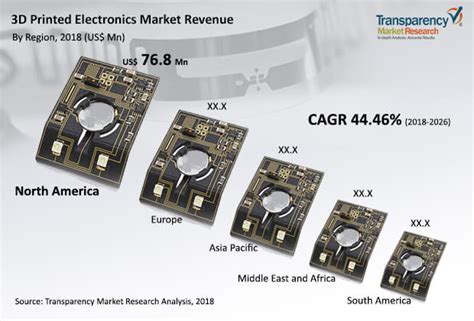
the promising and challenging future of 3d printed electronics
What are 3D-printed electronics? 3D-printed electronics involve using various additive manufacturing methods to deposit conductive, insulating, and semiconducting materials in precise patterns to create electronic[…]

product lifecycle management electronics manufacturing
What is PLM-EM? Product Lifecycle Management for Electronics Manufacturing (PLM-EM) is the application of PLM principles and software tools to manage the entire lifecycle of[…]
What PCB material do I need to use for RF
Understanding the Importance of PCB material selection in RF Design In RF applications, the PCB material plays a critical role in determining the electrical and[…]
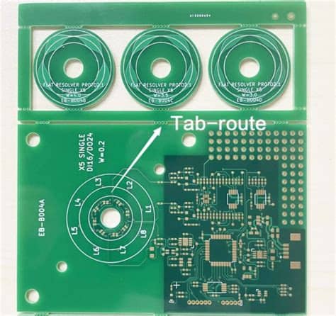
PCB Routing Tips for Beginners
Understanding the Basics of PCB Routing Before diving into the specifics of PCB routing, it’s essential to understand the basics. PCB routing involves creating the[…]
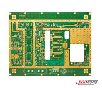
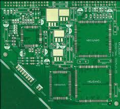
PCB Design Guideline
Understanding the Basics of PCB Design Before diving into the details of PCB design, it is essential to understand the basics. A PCB is a[…]
PCB Transmission Line: An Interconnection Between Transmitters and Receivers in a PCB
Introduction to PCB Transmission Lines In the world of electronics, the Printed Circuit Board (PCB) is a fundamental component that enables the interconnection and functionality[…]
PCB Schematic Design: in 10 einfachen Schritten zur Leiterplatte
Einführung in das PCB-Schematic-Design Das PCB-Schematic-Design ist der erste und wichtigste Schritt bei der Entwicklung einer Leiterplatte. Ein gut durchdachtes Schaltplan-Design bildet die Grundlage für[…]