What is a Castellated PCB?
A castellated PCB, also known as a castellated hole PCB or castellated edge PCB, is a printed circuit board that features plated semi-circular holes or slots along the edges. These castellations serve as a substitute for the traditional edge connector, enabling the board to be directly soldered to another PCB or surface. This unique design offers several advantages over conventional PCB Assembly methods, making castellated PCBs an increasingly popular choice for various electronic applications.
Key Features of Castellated PCBs
- Semi-circular holes or slots along the board edges
- Plated castellations for direct soldering
- Compatible with surface mount technology (SMT)
- Eliminates the need for additional connectors
- Facilitates compact and low-profile designs
Advantages of Using Castellated PCBs
Enhanced Mechanical Stability
One of the primary benefits of using castellated PCBs is the improved mechanical stability they offer. The plated castellations create a strong solder joint between the PCB and the connecting surface, ensuring a robust and reliable connection. This enhanced stability is particularly crucial in applications that are subject to vibration, shock, or other mechanical stresses.
Space Savings and Compact Designs
Castellated PCBs enable designers to create more compact and space-efficient electronic devices. By eliminating the need for additional connectors, castellated boards can be directly soldered to other PCBs or surfaces, resulting in a lower profile and reduced overall footprint. This is especially advantageous in modern electronic devices where space is at a premium, such as smartphones, wearables, and IoT devices.
| Traditional PCB Assembly | Castellated PCB Assembly |
|---|---|
| Requires connectors | Direct soldering |
| Increased board height | Lower profile |
| Larger footprint | Compact design |
Cost Reduction
Implementing castellated PCBs can lead to significant cost savings in the manufacturing process. By eliminating the need for separate connectors and the associated assembly steps, castellated boards streamline the production process and reduce the overall component count. This simplification results in lower material costs, reduced assembly time, and increased production efficiency.
Improved Signal Integrity
Castellated PCBs offer improved signal integrity compared to traditional connector-based assemblies. The direct solder connection between the castellated board and the mating surface minimizes signal loss and reduces the risk of signal reflections caused by impedance mismatches. This is particularly important in high-speed and high-frequency applications where signal integrity is critical.

Applications of Castellated PCBs
Castellated PCBs find applications in a wide range of industries and electronic devices. Some common examples include:
- IoT devices
- Wearable technology
- Smartphones and tablets
- Automotive electronics
- Medical devices
- Industrial control systems
- Aerospace and defense equipment

Designing Castellated PCBs
When designing castellated PCBs, several key considerations must be taken into account to ensure optimal performance and manufacturability.
Castellation Dimensions
The size and spacing of the castellations are critical factors in the design process. The castellation diameter should be large enough to accommodate the plating thickness and provide sufficient mechanical strength. The pitch, or distance between the centers of adjacent castellations, must be carefully chosen to ensure proper alignment and soldering with the mating surface.
| Castellation Parameter | Recommended Value |
|---|---|
| Diameter | 0.8 mm – 1.2 mm |
| Pitch | 1.27 mm – 2.54 mm |
| Plating Thickness | 25 μm – 50 μm |
Solder Mask Design
Proper solder mask design is essential for castellated PCBs. The solder mask should be applied to the castellations, leaving only the exposed copper areas for soldering. This selective masking helps to prevent solder bridging and ensures a clean and reliable solder joint. Additionally, the solder mask should be designed to provide adequate clearance around the castellations to facilitate inspection and rework if necessary.
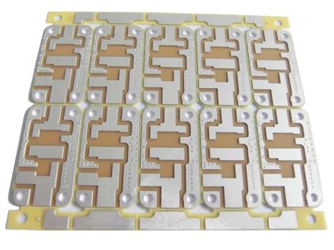
Panelization and Depanelization
Castellated PCBs are often manufactured in panels to increase production efficiency and reduce costs. The panelization process involves arranging multiple PCBs on a single panel, with castellations along the shared edges. After assembly, the individual boards are separated through a process called depanelization. Careful consideration must be given to the panelization layout and the depanelization method to ensure clean and accurate board separation without damaging the castellations or components.

Manufacturing Castellated PCBs
The manufacturing process for castellated PCBs involves several key steps to ensure high-quality and reliable boards.
-
PCB Fabrication: The PCB is manufactured using standard PCB fabrication techniques, including etching, drilling, and plating.
-
Castellation Formation: The castellations are created by drilling or routing semi-circular holes or slots along the board edges. The castellations are then plated to ensure good electrical conductivity and mechanical strength.
-
Solder Mask Application: The solder mask is selectively applied to the PCB, leaving the castellation areas exposed for soldering.
-
Surface Finish: A surface finish, such as ENIG (Electroless Nickel Immersion Gold) or HASL (Hot Air Solder Leveling), is applied to protect the exposed copper and enhance solderability.
-
Component Assembly: The electronic components are mounted on the castellated PCB using SMT processes, such as solder paste printing, component placement, and reflow soldering.
-
Inspection and Testing: The assembled castellated PCBs undergo thorough inspection and testing to ensure proper functionality, reliability, and compliance with quality standards.
Frequently Asked Questions (FAQ)
1. What are the main advantages of using castellated PCBs?
Castellated PCBs offer several advantages, including enhanced mechanical stability, space savings, cost reduction, and improved signal integrity. They enable compact and low-profile designs, eliminate the need for additional connectors, and provide a robust solder connection between the board and the mating surface.
2. Can castellated PCBs be used in high-reliability applications?
Yes, castellated PCBs are well-suited for high-reliability applications. The plated castellations create a strong and reliable solder joint, providing excellent mechanical stability and durability. Castellated boards are commonly used in aerospace, defense, medical, and automotive industries, where reliability is paramount.
3. How do I choose the appropriate castellation dimensions for my design?
When selecting castellation dimensions, consider factors such as the board thickness, component size, and the mating surface requirements. The castellation diameter should be large enough to accommodate the plating thickness and provide sufficient mechanical strength, typically ranging from 0.8 mm to 1.2 mm. The pitch, or distance between castellation centers, is usually chosen from standard values like 1.27 mm or 2.54 mm to ensure compatibility with common assembly processes.
4. Can castellated PCBs be assembled using standard SMT processes?
Yes, castellated PCBs are compatible with standard surface mount technology (SMT) assembly processes. The components can be mounted on the castellated board using solder paste printing, component placement, and reflow soldering techniques. The castellations themselves are soldered to the mating surface using similar SMT soldering methods.
5. Are there any specific design considerations for panelizing castellated PCBs?
When panelizing castellated PCBs, it’s essential to consider the board layout, component placement, and depanelization method. The panelization layout should ensure adequate spacing between individual boards to prevent damage during depanelization. The depanelization process, such as V-scoring or tab routing, should be carefully selected to ensure clean and accurate board separation without damaging the castellations or components. Additionally, the panelization design should account for any specific manufacturing or assembly requirements, such as tooling holes or fiducial marks.
Conclusion
Castellated PCBs offer a compelling solution for assembling compact, reliable, and cost-effective electronic devices. By leveraging the advantages of direct soldering and eliminating the need for additional connectors, castellated boards enable space savings, improved signal integrity, and enhanced mechanical stability. With careful design considerations and proper manufacturing processes, castellated PCBs can be successfully implemented in a wide range of applications across various industries.
As technology continues to advance and the demand for miniaturization and high-performance electronics grows, castellated PCBs are poised to play an increasingly important role in shaping the future of electronIC Packaging and assembly.
No responses yet