What are PCBs?
PCBs are the backbone of modern electronics. They are flat boards made of insulating materials, such as fiberglass or plastic, with conductive copper traces printed on them. These traces connect various electronic components, such as resistors, capacitors, and integrated circuits, to form a complete electronic circuit.
PCBs offer several advantages over traditional point-to-point wiring:
- Compact design
- Improved reliability
- Easier mass production
- Reduced electromagnetic interference (EMI)
Why Create Your Own PCBs?
There are several reasons why you might want to create your own PCBs:
-
Customization: By designing your own PCBs, you have complete control over the layout, component selection, and functionality of your electronic project.
-
Cost savings: For small-scale projects or prototypes, creating your own PCBs can be more cost-effective than ordering them from a professional manufacturer.
-
Learning experience: Designing and fabricating your own PCBs is an excellent way to learn about electronics, circuit design, and manufacturing processes.
-
Rapid prototyping: With the right tools and resources, you can quickly iterate on your designs and create working prototypes in a matter of days.

The PCB Design Process
Step 1: Schematic Design
The first step in creating a custom PCB is to design the schematic. A schematic is a graphical representation of the electronic circuit, showing how the various components are connected. There are several software tools available for schematic design, such as:
- KiCad (open-source)
- Eagle (free for non-commercial use)
- Altium Designer (paid)
When designing your schematic, consider the following:
- Component selection
- Power supply requirements
- Signal integrity
- Electromagnetic compatibility (EMC)
Step 2: PCB Layout
Once your schematic is complete, you can move on to the PCB layout. This involves arranging the components on the board and routing the copper traces to connect them according to the schematic. PCB layout software, such as those mentioned above, can help you with this process.
When laying out your PCB, keep in mind:
- Component placement for optimal signal flow
- Trace width and spacing for signal integrity and manufacturability
- Ground planes for EMI reduction and power distribution
- Mounting holes and mechanical constraints
Step 3: Fabrication
After finalizing your PCB layout, you can proceed with fabrication. There are two main options for DIY PCB fabrication:
-
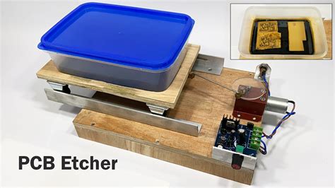
Etching: This involves printing your PCB layout onto a transparent film, exposing it onto a photosensitive copper-clad board, and then etching away the unwanted copper using a chemical solution. This method is suitable for simple, single-layer designs and can be done at home with minimal equipment.
-
PCB milling: This process uses a small CNC (Computer Numerical Control) machine to mill away the unwanted copper from a copper-clad board, leaving behind the desired traces. PCB milling is more precise than etching and can handle double-sided designs, but it requires specialized equipment.
If you don’t want to fabricate your PCBs yourself, you can also use online PCB manufacturing services, such as:
- OSH Park
- JLCPCB
- PCBWay
These services offer affordable, high-quality PCB fabrication with quick turnaround times.
Step 4: Assembly
Once your PCBs are fabricated, it’s time to assemble the components. This can be done by hand using a soldering iron or with the help of a pick-and-place machine for surface-mount components.
When assembling your PCBs, consider:
- Component orientation
- Soldering techniques (e.g., through-hole, surface-mount)
- Electrostatic discharge (ESD) precautions
- Testing and debugging

Tools and Resources for DIY PCBs
To get started with DIY PCBs, you’ll need some essential tools and resources:
-
Schematic and PCB layout software: As mentioned earlier, KiCad, Eagle, and Altium Designer are popular options.
-
Fabrication equipment: For etching, you’ll need a UV exposure unit, etchant solution, and a drill press. For PCB milling, you’ll need a small CNC machine and milling bits.
-
Soldering equipment: A soldering iron, solder, flux, and a fume extractor are essential for assembling your PCBs.
-
Components: You’ll need a variety of electronic components, such as resistors, capacitors, and integrated circuits, depending on your project requirements.
-
Online resources: There are numerous online communities, forums, and tutorials dedicated to DIY PCBs. Some popular ones include:
- EEVblog
- Hackaday
- Instructables
- SparkFun Electronics

Table: Comparison of DIY PCB Fabrication Methods
| Method | Pros | Cons |
|---|---|---|
| Etching | – Low cost | – Limited to single-layer designs |
| – Can be done at home with minimal equipment | – Requires handling of hazardous chemicals | |
| – Suitable for simple designs | – Lower precision compared to PCB milling | |
| PCB Milling | – Higher precision than etching | – Requires specialized CNC equipment |
| – Can handle double-sided designs | – Higher cost than etching | |
| – No hazardous chemicals involved | – Milling bits wear out and need to be replaced | |
| Online Services | – High-quality, professional-grade PCBs | – Higher cost than DIY methods for small quantities |
| – Quick turnaround times | – Limited customization options | |
| – No need for personal fabrication equipment | – Shipping time and costs |
Frequently Asked Questions (FAQ)
-
Q: How much does it cost to make your own PCBs?
A: The cost of making your own PCBs depends on the fabrication method and the components used. Etching is generally the most affordable option, with material costs ranging from a few dollars to around $50 for a simple project. PCB milling requires a higher initial investment in equipment but can be more cost-effective in the long run. Online PCB manufacturing services typically charge around $5-$10 per square inch for small quantities. -
Q: What is the minimum trace width and spacing for DIY PCBs?
A: The minimum trace width and spacing depend on the fabrication method and the capabilities of your equipment. For etching, a minimum trace width of 0.2mm (8mil) and a spacing of 0.2mm (8mil) is achievable with careful work. PCB milling can achieve trace widths and spacings down to 0.1mm (4mil) or lower, depending on the machine and milling bits used. -
Q: Can I create multi-layer PCBs at home?
A: Creating multi-layer PCBs at home is more challenging than single or double-sided designs. Etching is not suitable for multi-layer PCBs, as it cannot create the necessary interconnects between layers. Some advanced PCB milling machines can handle multi-layer designs, but they are more expensive and require specialized software and skills. -
Q: What are some common mistakes to avoid when designing PCBs?
A: Some common mistakes to avoid when designing PCBs include: - Not considering component placement and signal flow during layout
- Using traces that are too narrow or too close together, leading to manufacturing issues or signal integrity problems
- Forgetting to include mounting holes or mechanical constraints
- Not properly grounding the circuit or using inadequate power distribution
-
Neglecting to test and debug the assembled PCB
-
Q: How long does it take to design and fabricate a custom PCB?
A: The time required to design and fabricate a custom PCB varies depending on the complexity of the project and the fabrication method used. A simple, single-layer PCB can be designed in a few hours and etched at home within a day. More complex designs may take several days to a week for design and fabrication. Using online PCB manufacturing services typically adds a few days to a week for production and shipping.
Conclusion
Creating your own custom PCBs is a rewarding and educational experience for anyone interested in electronics. With the right tools, resources, and knowledge, you can bring your electronic projects to life and explore the fascinating world of PCB design and fabrication.
Remember to start with simple designs, follow best practices for schematic and layout design, and choose the fabrication method that best suits your needs and skills. Don’t be afraid to experiment, learn from your mistakes, and seek help from the vibrant online community of PCB enthusiasts.
Happy PCB making!
No responses yet