Introduction to Flex-Rigid Routing
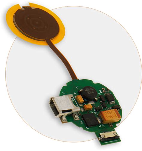
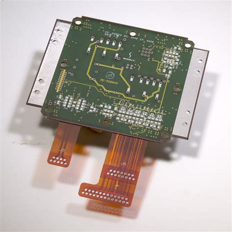
Flex-rigid routing refers to the process of creating electrical connections between flexible and rigid regions on a printed circuit board (PCB). This type of routing presents unique challenges compared to routing on a fully rigid board due to the differences in material properties and the need for the flex region to bend and move.
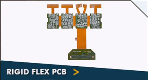
Flex-rigid PCBs combine the benefits of both rigid and flexible substrates, allowing for more compact and adaptable designs. The rigid regions provide structural support and allow for the mounting of components, while the flexible regions enable the board to fold, twist, or conform to the available space.
However, routing traces between the flex and rigid regions can be problematic. The transition point where the two materials meet is a potential weak spot susceptible to stress and fatigue. Improper routing techniques can lead to signal integrity issues, mechanical failures, and reduced reliability.
In this article, we will explore the challenges of flex-rigid routing, best practices for overcoming these challenges, and troubleshooting tips for when you encounter the dreaded “can’t route between flex and rigid regions” error.
Challenges of Flex-Rigid Routing
Different Material Properties
One of the primary challenges in flex-rigid routing stems from the different material properties of the flexible and rigid substrates. Flexible materials, such as polyimide, have different thermal expansion coefficients, dielectric constants, and mechanical characteristics compared to rigid FR-4 materials.
These differences can lead to issues like:
- Mismatched thermal expansion: As the temperature changes, the flex and rigid regions may expand and contract at different rates, causing stress on the traces and solder joints.
- Impedance discontinuities: The dielectric constant of the flexible material may differ from the rigid material, leading to impedance mismatches that can affect signal integrity.
- Mechanical stress: The repeated bending and flexing of the flex region can put mechanical stress on the traces, potentially causing them to crack or break over time.
Bending and Flexing
The ability of the flex region to bend and move is both an advantage and a challenge for routing. While the flexibility allows for more design freedom, it also introduces additional considerations:
- Bend radius: The traces on the flex region must be able to withstand the expected bend radius without breaking or experiencing excessive stress. The minimum bend radius depends on factors like the thickness of the flex material, the copper weight, and the number of layers.
- Fatigue: Repeated bending and flexing can cause fatigue in the traces, leading to cracks and failures over time. The routing pattern and the use of strain relief techniques can help mitigate this issue.
- Creep: The flexible material may experience creep, where it slowly deforms over time under constant stress. This can cause the traces to shift or deform, potentially leading to shorts or opens.
Transition Points
The transition points where the flex and rigid regions meet are critical areas that require special attention during routing. These transition points are subject to stress concentrations and are prone to failures if not designed properly.
Challenges at the transition points include:
- Stress concentration: The abrupt change in material properties at the transition point can cause stress to concentrate in a small area, increasing the risk of fatigue and failure.
- Adhesion: Ensuring good adhesion between the flex and rigid materials is crucial to prevent delamination and maintain the integrity of the traces.
- Alignment: Misalignment between the flex and rigid layers can cause issues like poor connection, shorts, or opens.
Best Practices for Flex-Rigid Routing
To overcome the challenges of flex-rigid routing and ensure a reliable and robust design, follow these best practices:
Material Selection
Choose materials that are compatible and well-suited for flex-rigid applications. Consider factors like:
- Flexible substrate: Select a flexible substrate material, such as polyimide, that has good mechanical and electrical properties, and can withstand the expected environmental conditions.
- Adhesives: Use adhesives that provide strong bonding between the flex and rigid materials, and can tolerate the expected stress and strain.
- Copper weight: Choose the appropriate copper weight for the traces based on the current requirements and the expected bend radius. Thicker copper can provide better conductivity but may be more prone to cracking when flexed.
Routing Techniques
Employ routing techniques that minimize stress and improve reliability:
- Curved traces: Use curved traces instead of sharp corners to reduce stress concentrations and improve flexibility. Avoid acute angles and abrupt changes in direction.
- Strain relief: Incorporate strain relief techniques, such as accordion-shaped or “S”-shaped traces, to allow for some movement and reduce stress on the traces during flexing.
- Staggered traces: Stagger the traces at the transition points to distribute the stress more evenly and prevent all the traces from being subjected to the same stress at the same location.
- Hatched polygons: Use hatched polygons for large copper areas to improve flexibility and reduce the risk of cracking.
Transition Point Design
Pay special attention to the design of the transition points:
- Gradual transition: Create a gradual transition between the flex and rigid regions to minimize stress concentrations. Use techniques like beveling or stepping to create a smoother transition.
- Reinforcement: Reinforce the transition points with additional material, such as coverlay or stiffeners, to provide extra support and reduce the risk of delamination.
- Alignment: Ensure precise alignment between the flex and rigid layers to maintain the integrity of the traces and prevent shorts or opens.
Testing and Validation
Thoroughly test and validate the flex-rigid design to ensure its reliability and performance:
- Mechanical testing: Perform mechanical tests, such as bend and twist tests, to verify that the design can withstand the expected stress and strain without failure.
- Thermal cycling: Conduct thermal cycling tests to assess the design’s ability to handle temperature variations and the resulting thermal expansion and contraction.
- Signal integrity: Validate the signal integrity of the design through simulations and measurements to ensure that the traces maintain the required impedance and avoid issues like reflections or crosstalk.

Troubleshooting “Can’t Route Between Flex and Rigid Regions” Errors
If you encounter the “can’t route between flex and rigid regions” error during the design process, here are some troubleshooting tips:
-
Check the layer stack-up: Ensure that the layer stack-up is properly defined, and the flex and rigid regions are correctly assigned. Verify that the transition layers are properly configured.
-
Verify the design rules: Check that the design rules, such as minimum trace width, spacing, and bend radius, are properly set and adhered to in the design. Adjust the rules if necessary to accommodate the specific requirements of the flex-rigid design.
-
Inspect the transition points: Carefully examine the transition points between the flex and rigid regions. Look for any design issues, such as abrupt transitions, insufficient clearance, or misalignment between layers. Modify the design to create smoother transitions and ensure proper alignment.
-
Review the routing pattern: Analyze the routing pattern in the flex region. Look for areas where the traces may be experiencing excessive stress or violating the bend radius rules. Adjust the routing pattern to incorporate strain relief techniques and minimize stress concentrations.
-
Optimize the component placement: Consider the placement of components near the transition points. Ensure that the components are not too close to the transition, which can cause stress on the traces. Adjust the component placement to provide adequate clearance and reduce stress.
-
Verify the copper balance: Check the copper balance in the flex and rigid regions. Unbalanced copper distribution can cause warpage and stress issues. Ensure that the copper is evenly distributed and consider adding copper balancing features if necessary.
-
Consult with the manufacturer: If the error persists, consult with the flex-rigid PCB manufacturer for guidance and recommendations. They may have specific guidelines or requirements for their manufacturing process that can help resolve the routing issues.
Flex-Rigid Routing FAQs
1. What is the minimum bend radius for flex-rigid PCBs?
The minimum bend radius for flex-rigid PCBs depends on several factors, including the thickness of the flexible material, the copper weight, and the number of layers. As a general rule of thumb, the minimum bend radius should be at least 6 times the total thickness of the flex region. However, it’s essential to consult with the manufacturer and follow their specific guidelines for the chosen materials and stack-up.
2. Can I use the same design rules for flex and rigid regions?
No, the design rules for flex and rigid regions are typically different due to the unique requirements and characteristics of each material. The flex region may require different trace widths, spacings, and bend radii compared to the rigid region. It’s important to define separate design rules for the flex and rigid regions to ensure manufacturability and reliability.
3. How can I reduce stress on the traces in the flex region?
To reduce stress on the traces in the flex region, consider the following techniques:
- Use curved traces instead of sharp corners to minimize stress concentrations.
- Incorporate strain relief features, such as accordion-shaped or “S”-shaped traces, to allow for some movement and reduce stress during flexing.
- Stagger the traces at the transition points to distribute the stress more evenly.
- Use hatched polygons for large copper areas to improve flexibility and reduce the risk of cracking.
- Ensure that the bend radius of the traces is within the recommended limits for the chosen materials and stack-up.
4. What are some common causes of delamination in flex-rigid PCBs?
Delamination in flex-rigid PCBs can occur due to several reasons, including:
- Poor adhesion between the flex and rigid materials.
- Excessive stress or strain at the transition points.
- Inadequate design of the transition regions, such as abrupt changes in material properties or insufficient reinforcement.
- Thermal mismatch between the flex and rigid materials, causing stress during temperature changes.
- Improper handling or assembly processes that introduce stress or damage to the laminated areas.
To minimize the risk of delamination, ensure good adhesion between the materials, design smooth transitions, reinforce the transition points, and follow proper handling and assembly procedures.
5. How can I ensure signal integrity in flex-rigid PCBs?
To ensure signal integrity in flex-rigid PCBs, consider the following guidelines:
- Choose materials with compatible dielectric constants to minimize impedance discontinuities between the flex and rigid regions.
- Control the impedance of the traces by adjusting the trace width, spacing, and dielectric thickness.
- Use ground planes and proper shielding techniques to reduce crosstalk and electromagnetic interference (EMI).
- Minimize the length of traces in the flex region to reduce signal loss and attenuation.
- Perform signal integrity simulations and measurements to validate the design and identify any potential issues.
- Follow best practices for high-speed design, such as minimizing vias, using differential pairs, and managing return paths.
Conclusion
Flex-rigid routing presents unique challenges due to the different material properties, bending and flexing requirements, and critical transition points. By understanding these challenges and following best practices for material selection, routing techniques, and transition point design, designers can overcome the “can’t route between flex and rigid regions” error and create reliable and high-performance flex-rigid PCBs.
Thorough testing and validation, including mechanical, thermal, and signal integrity tests, are essential to ensure the robustness and reliability of the flex-rigid design. When troubleshooting routing issues, designers should review the layer stack-up, design rules, transition points, routing pattern, component placement, and copper balance to identify and resolve any problems.
By leveraging the advantages of flex-rigid technology and adhering to proven design guidelines, designers can create innovative and reliable products that meet the demands of today’s increasingly complex and compact electronic devices.
No responses yet