QFN Package Overview
QFN packages have a leadless design where the contact pads are located on the bottom surface of the component body. This allows for a very compact footprint. Typical sizes range from 1x1mm to 12x12mm with anywhere from 4 to over 100 contact pads.
Some key characteristics of QFN packages include:
- Leadless contacts on bottom of package
- Exposed die-attach paddle for enhanced thermal dissipation
- Thin package profile, typically 0.75mm or less
- Fine lead pitch, commonly 0.4mm, 0.5mm or 0.65mm
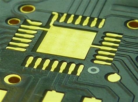
QFN Pad Layout
The PCB footprint for a QFN consists of peripheral contact pads and usually a central thermal pad. A typical QFN footprint is shown below:
| Element | Description |
|---|---|
| Contact pads | Rectangular pads on edges of footprint corresponding to package contacts |
| Thermal pad | Large central pad for package die-attach paddle |
| Vias | Plated through-holes connecting thermal pad to inner plane layers |
Contact pads are typically non-solder mask defined (NSMD), meaning the copper extending to the edge of the mask opening. This maximizes the usable area for solder fillet formation.
The thermal pad is also typically NSMD but with a larger mask opening than the copper area. A 50% larger opening on each side is a common rule of thumb. So for a 3x3mm thermal pad, the mask opening would be 3.5×3.5mm.
Thermal Pad and Vias
A key aspect of the QFN footprint is the central thermal pad. Its large size relative to the contacts enables efficient heat transfer from the die to the board. Connecting it to inner copper plane layers with vias further enhances heat spreading.
The size and number of thermal vias is a tradeoff between thermal dissipation and board real estate. More vias provide a lower thermal resistance path but also take up more routing space. A typical strategy is placing vias in a grid pattern with 1.0-1.2mm via pitch.
Via size should be as large as possible while still allowing sufficient space between vias for solder wicking. 0.3-0.33mm drill with 0.7mm pad size is common. Filled or capped vias are preferred to prevent solder theft.
PCB Design Guidelines for QFN Soldering
Proper footprint design is critical for successful QFN soldering. The following guidelines help ensure robust solder joints.
Pad Size and Spacing
Contact pads should be sized to provide sufficient area for a strong solder fillet while allowing some placement tolerance. A typical recommendation is making pads 0.2-0.35mm longer than the package contact length.
Pad width should closely match the contact width, with no more than 0.05mm side overhang to prevent bridging. For finer-pitch QFNs, a narrower pad may be used to increase clearance between pads.
Pad spacing is dictated by the package drawing. Typical minimum values are:
| Pitch (mm) | Pad Spacing (mm) |
|---|---|
| 0.4 | 0.2 |
| 0.5 | 0.3 |
| 0.65 | 0.4 |
Soldermask Clearance
As mentioned, an NSMD pad configuration is preferred for QFNs. The mask opening should be sized to maximize the exposed copper area while preventing bridging between pads.
A mask expansion of 0.05-0.075mm per side is typical, resulting in 0.1-0.15mm wider mask opening than the copper. The mask dam between pads should be a minimum of 0.1mm to avoid bridging.
For the thermal pad, a larger mask opening is used to allow outgassing of volatiles during reflow. 1.5-2x the pad size is typical. So a 0.25mm mask expansion per side for a 0.5mm opening.
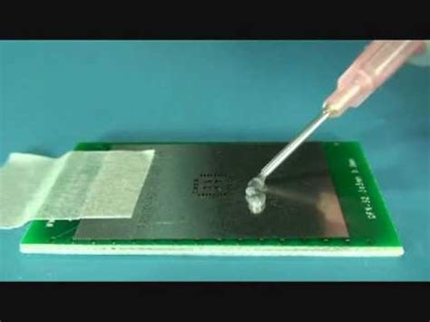
Solderpaste Stencil Design
Proper solderpaste volume is crucial for reliable QFN joints. Insufficient paste can lead to open circuits while excess promotes bridging.
Stencil aperture size should match the copper pad size 1:1. The exception is pads at the package corner which may be reduced to 75-80% to avoid paste overflow.
For fine-pitch QFNs (<0.5mm), aperture size may need to be reduced to 90-95% of pad size to prevent bridging. In this case a thinner stencil foil (0.1mm) and Type 4 or Type 5 paste are recommended.
The thermal pad aperture should cover 50-80% of the pad area to balance solder volume and paste release. An array of smaller square or hexagonal openings is preferred over one large opening. 2-3mm aperture size with 0.5mm spacing between apertures is typical.
Via-in-Pad
Vias placed in the thermal pad can be problematic for soldering. The via hole can wick solder away from the joint, resulting in a starved connection.
Plugged or filled vias are recommended wherever possible. Conductive via fill materials such as conductive epoxy or sintered silver paste are preferred for their thermal conductivity. Non-conductive filling with epoxy or resin also works but has higher thermal resistance.
If open vias must be used, tenting the vias with soldermask on the component side can help minimize solder theft. The mask should cover 50-75% of the via circumference. Reducing via size also helps – 0.2-0.25mm drill size is recommended.
Assembly Process Considerations
In addition to layout, the assembly process for QFNs must be carefully controlled to achieve reliable joints. Key factors include:
Solderpaste Selection
Type 3 or higher (smaller particle size) solderpaste is recommended for QFNs, especially <0.5mm pitch. The finer particles enable printing of smaller, well-defined deposits.
No-clean pastes are preferred to avoid residue entrapment under the low standoff package. If cleaning is required, select a paste compatible with the cleaning process and ensure complete residue removal.
Reflow Profile
A reflow profile with a relatively long preheat and peak temperature 10-20°C above liquidus is recommended for QFNs. This ensures complete solder melting and wetting under the confined space of the package.
Nitrogen atmosphere reflow is beneficial for fine-pitch QFNs. N2 reduces oxidation of the paste and pad surfaces, promoting better coalescence and a lower defect rate.
Inspection and Rework
Transmission X-ray is the preferred method for inspecting QFN solder joints due to the hidden joints under the package. 2D X-ray can detect gross defects like bridging and insufficient solder. 3D or CT X-ray enables measurement of joint volume and detection of subtler defects like voids.
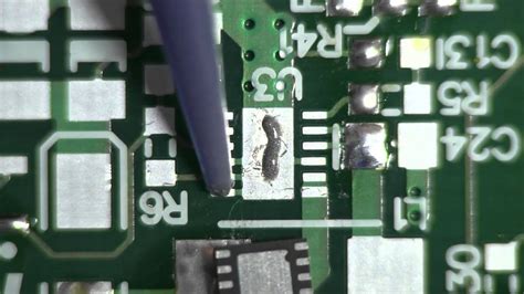
If rework is necessary, a hot air reflow system with localized heating nozzle is recommended. Precise temperature control and a controlled heating rate is important to avoid thermal damage. After package removal, the pads should be cleaned of residual solder before reprinting paste and installing a new package.

Summary
QFN packages offer many benefits but require careful PCB layout for reliable soldering. Key aspects include:
- NSMD pad definition for maximized soldering area
- Thermal pad with multiple vias for heat dissipation
- Adequate soldermask clearances to prevent solder bridging
- Optimized solderpaste stencil aperture design
- Filled or capped vias to prevent solder wicking
- Type 3 or higher paste for fine pitches
- Controlled reflow profile and atmosphere
- X-ray inspection and localized rework
By following these guidelines, designers and assemblers can achieve high-yield, robust solder joints when using QFN packages.
FAQ
What is the typical pad size for a QFN contact?
Pads are usually 0.2-0.35mm longer than the package contact length, and equal in width or slightly narrower (0.05mm or less per side).
How much soldermask clearance is needed between QFN pads?
A mask expansion of 0.05-0.075mm per side is typical, providing a minimum 0.1mm dam between pads to prevent bridging.
What type of solderpaste is best for fine-pitch QFNs?
Type 3 or higher (smaller particle size) paste enables printing well-defined deposits for pitches less than 0.5mm. No-clean formulations are preferred to avoid residue under the low-standoff package.
Why are filled vias recommended for the QFN thermal pad?
Filling vias with a conductive or non-conductive material prevents solder wicking away from the thermal pad joint. This is especially problematic for vias located directly under the package.
How are QFN solder joints inspected?
Transmission X-ray is the most effective method to inspect the hidden solder joints under a QFN. 2D X-ray detects gross defects while 3D/CT X-ray allows measurement of joint volume and more subtle defects.
No responses yet