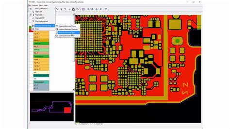
pcb gerber viewer
Introduction to PCB Gerber Viewers PCB (Printed Circuit Board) design is a complex process that involves multiple steps, from schematic capture to PCB layout and[…]
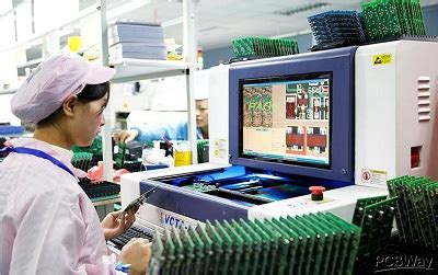
pcb functional testing and role manufacturer collaboration
Introduction to PCB Testing Printed Circuit Board (PCB) testing is a crucial step in the electronics manufacturing process to ensure the quality, reliability, and functionality[…]
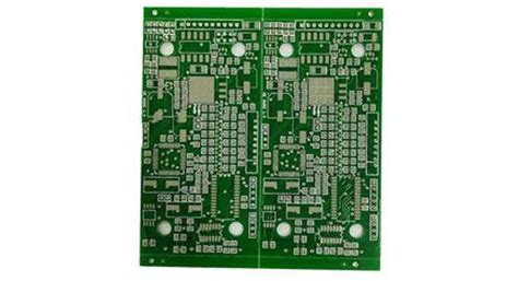
pcb fabrication drawing
Introduction to PCB Fabrication Printed Circuit Board (PCB) fabrication is a complex process that involves multiple steps and requires precise planning and execution. One of[…]
eliminate emi problems design stage robust emi design rule check plane resonance analysis
Introduction to EMI and its Impact on Electronic Systems Electromagnetic interference (EMI) is a major concern in the design and development of electronic systems. EMI[…]
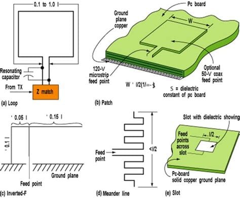
dual band pcb antenna design keeping your emi line
Introduction to PCB Antenna Design Printed Circuit Board (PCB) antennas have become increasingly popular in modern wireless communication devices due to their compact size, low[…]
Steps In PCB Fabrication Process PCB Manufacturing technique
Introduction to PCB fabrication Printed Circuit Boards (PCBs) are the backbone of modern electronics. They provide a platform for electrical components to be mounted and[…]
Why is RAYPCB production resumed much faster than its competitors
RAYPCB’s agile manufacturing process enables fast resumption of PCB production In the fast-paced world of electronic manufacturing, the ability to quickly resume production after interruptions[…]
PCB Edge Clearance
What is PCB edge clearance and Why is it Important? PCB edge clearance refers to the minimum distance that must be maintained between the edge[…]
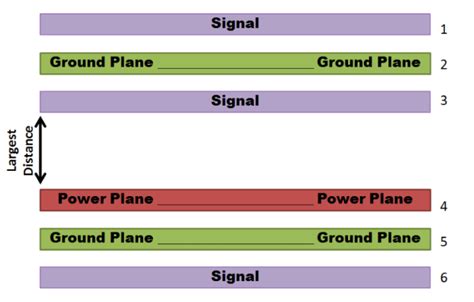
pcb layer stack
What is a PCB Layer Stack? A printed circuit board (PCB) layer stack refers to the arrangement and configuration of the various layers that make[…]
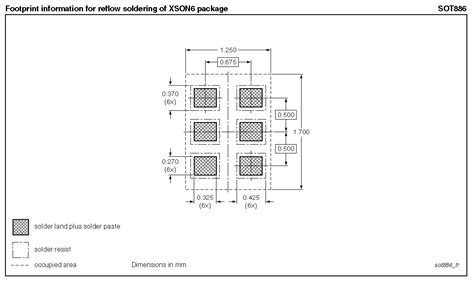
pcb land pattern design ipc 7351 standard
Introduction to PCB Land Patterns and the IPC-7351 Standard Printed Circuit Board (PCB) design is a complex process that involves various aspects, one of which[…]