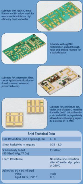
What Is Copper Clad Laminate CCL
Composition and Structure of Copper Clad Laminate Copper Foil Layer The copper foil layer in CCL is typically made of high-purity, electrodeposited copper. The thickness[…]
Why is controlled impedance so important
Introduction to Controlled Impedance Controlled impedance is a crucial concept in the realm of electronics and Electrical Engineering. It refers to the precise management of[…]
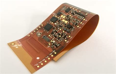
Why use rigid flex PCB than flexible PCB in electronic project
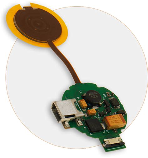
Introduction to Rigid-flex PCB Rigid-flex PCBs are a hybrid design that combines the benefits of both rigid and flexible printed circuit boards. This innovative technology[…]
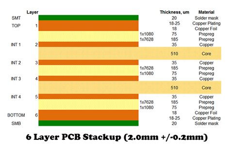
PCB Layer stack up
What is PCB Layer Stack Up? A PCB (Printed Circuit Board) layer stack up refers to the arrangement of copper layers and insulating materials that[…]

Background Turns Dark When Placing Track
Understanding the Track-Darkening Phenomenon When working with audio or video editing software, you may have encountered a peculiar issue where the background of your project[…]

Can I Increase The Quality Of The Decals In Solidworks Mcad
Understanding Decals in SolidWorks Before we dive into the techniques for improving decal quality, let’s first understand what decals are and how they work in[…]
Cannot Select A Object That Somehow Is Very Far From Pcb Boundary
Understanding PCB Boundary Selection PCB (Printed Circuit Board) design involves placing various components and objects within a defined boundary. The PCB boundary represents the physical[…]
Can T Connect To Altium Infrastructure Server Ais After Installation
Understanding the Altium Infrastructure Server Before diving into troubleshooting, it’s important to understand what the Altium Infrastructure Server is and how it fits into your[…]
Can T Route Between Flex And Rigid Regions
Introduction to Flex-Rigid Routing Flex-rigid routing refers to the process of creating electrical connections between flexible and rigid regions on a printed circuit board (PCB).[…]
Clearance Constrain Between Polyregion On Multilayer And Pad On Top Layer
Introduction to Polyregion-Pad Clearance When designing multilayer printed circuit boards (PCBs), it’s critical to maintain proper clearance between copper areas on different layers to avoid[…]