Types of Filters – A Comprehensive Guide
Table of Contents Introduction to Filters Mechanical Filters Depth Filters Surface Filters Strainers Chemical Filters Activated Carbon Filters Ion Exchange Filters Catalytic Filters Biological Filters[…]
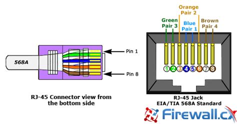
Rj45 Connector Pinouts: A Complete Guide and More!
Introduction to Rj45 Pinouts The RJ45 connector is the standard connector used for Ethernet networking. It is an 8-position, 8-contact (8P8C) connector that is commonly[…]
Circuits With Free Energy: Is it Possible to Make Free Energy?
What Are Free-Energy Circuits? Free-energy circuits, also known as over-unity devices or perpetual motion machines, are hypothetical electrical circuits that claim to generate more energy[…]
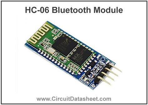
Hc06 Datasheet: Introduction to Pinout, Features, Applications, and Working Principle
What is the Hc06 Bluetooth Module? The Hc06 is a compact, low-cost, and easy-to-use Bluetooth module designed for wireless serial communication. It is based on[…]
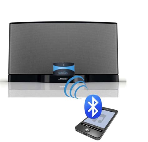
How To Tell If My Computer Has Bluetooth
What is Bluetooth Compatibility? Bluetooth is a wireless technology standard used for exchanging data between fixed and mobile devices over short distances. Bluetooth compatibility refers[…]
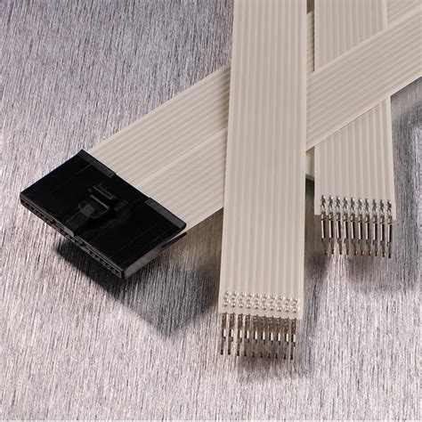
Flexible Flat Cable – How to Make your Designs More Innovative?
What is Flexible Flat Cable? Flexible flat cable, also known as FFC, is a type of electrical cable that is designed to be thin, lightweight,[…]
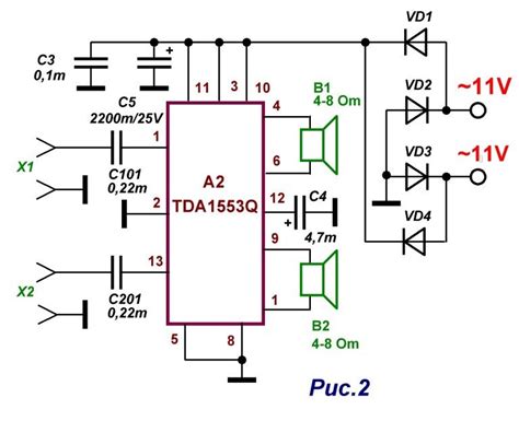
TDA1554Q Comprehensive Circuit Overview
Introduction to the TDA1554Q The TDA1554Q is a quad power amplifier IC designed for car audio applications. It is capable of delivering high power output[…]
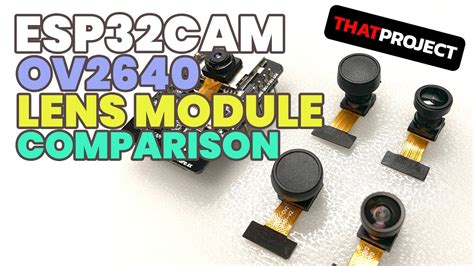
OV2640 – The Ultimate Guide on the Image Sensor
Introduction to OV2640 The OV2640 is a popular image sensor widely used in various applications, including IoT devices, security cameras, and embedded systems. Developed by[…]
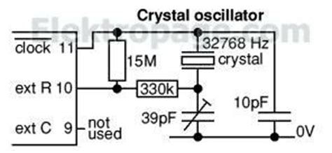
IC 4060: Understanding the Pinout and their Functions
Introduction to IC 4060 Pinout The IC 4060, also known as the CD4060 or HCF4060, is a 14-stage ripple carry binary counter integrated circuit. It[…]
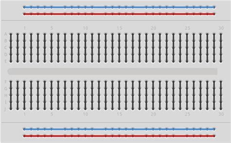
Breadboard Connections: An Introductory Guide
What is a Breadboard? A breadboard is a fundamental tool used in electronics prototyping and circuit design. It is a rectangular plastic board with numerous[…]