Introduction to Blind Via PCB
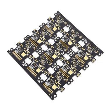
Blind via PCBs have become increasingly popular in the electronics industry due to their ability to maximize space utilization and improve overall circuit performance. In this comprehensive article, we will delve into the world of blind via PCBs, exploring their definition, advantages, manufacturing process, design considerations, applications, and future trends. By the end of this article, you will have a thorough understanding of blind via PCBs and their significance in the ever-evolving world of electronics.
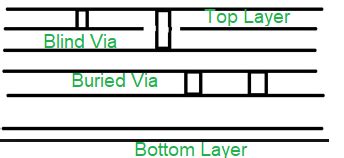
What is a Blind Via PCB?
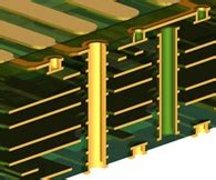
A blind via is a type of interconnect that connects an outer layer to one or more inner layers, but does not penetrate through the entire thickness of the PCB. Unlike through-hole vias, which are visible on both sides of the board, blind vias are only visible on one side. This unique characteristic allows for more efficient use of board space and enables the creation of high-density designs.
Advantages of Blind Via PCBs
Blind via PCBs offer several advantages over traditional PCB designs:
-
Space Savings: By utilizing blind vias, designers can place components closer together, resulting in smaller overall board sizes and more compact devices.
-
Improved Signal Integrity: Blind vias reduce the length of signal paths, minimizing signal loss and improving overall signal integrity.
-
Enhanced Thermal Management: Blind vias can be used to create thermal vias, which help dissipate heat from high-power components, improving the thermal performance of the PCB.
-
Increased Routing Flexibility: With blind vias, designers have more flexibility in routing traces, as they can be placed in areas that would otherwise be inaccessible with through-hole vias.
Manufacturing Process of Blind Via PCBs
The manufacturing process for blind via PCBs is more complex than that of standard PCBs, requiring specialized equipment and techniques. Here are the key steps involved:
Step 1: Layer Stack-up Design
The first step in manufacturing a blind via PCB is to design the layer stack-up. This involves determining the number of layers, their arrangement, and the placement of blind vias. The stack-up design must take into account the electrical requirements, material properties, and manufacturing capabilities.
Step 2: Drilling Blind Vias
Once the layer stack-up is finalized, the next step is to drill the blind vias. This process requires specialized equipment, such as laser drills or controlled depth drilling machines, to create precise and consistent blind vias. The depth of the blind vias is carefully controlled to ensure proper connection to the desired inner layers.
Step 3: Plating and Filling Blind Vias
After drilling, the blind vias are plated with a conductive material, typically copper, to establish electrical connections between the layers. In some cases, the blind vias may also be filled with a non-conductive material to improve structural integrity and prevent moisture ingress.
Step 4: Lamination and Pressing
The drilled and plated layers are then laminated together using heat and pressure. This process bonds the layers together, creating a solid and stable PCB structure. The pressing process ensures that the layers are properly aligned and free from any air gaps or voids.
Step 5: Outer Layer Processing
Once the lamination is complete, the outer layers of the PCB are processed. This includes applying the copper foil, patterning the circuit traces, and applying the solder mask and silkscreen. The blind vias are now hidden within the structure of the PCB, with only their openings visible on the outer layers.
Design Considerations for Blind Via PCBs
Designing a blind via PCB requires careful consideration of several factors to ensure optimal performance and manufacturability. Some key design considerations include:
Via Size and Spacing
The size and spacing of blind vias are critical factors in PCB design. Smaller via sizes allow for higher density layouts but may pose manufacturing challenges. It is essential to work closely with the PCB manufacturer to determine the minimum via size and spacing that can be reliably produced.
Via Aspect Ratio
The aspect ratio of a blind via refers to the ratio of its depth to its diameter. High aspect ratio vias are more challenging to manufacture and may require specialized processes. Designers must consider the aspect ratio limitations of the manufacturing process when designing blind via PCBs.
Layer Stack-up Optimization
Optimizing the layer stack-up is crucial for achieving the desired electrical performance and signal integrity. Factors such as dielectric thickness, copper weight, and layer arrangement must be carefully considered to minimize signal loss, crosstalk, and impedance mismatches.
Thermal Management
Blind vias can be used to create thermal vias, which help dissipate heat from high-power components. Designers must strategically place thermal vias to ensure effective heat transfer and prevent thermal hotspots on the PCB.
DFM Analysis
Design for Manufacturability (DFM) analysis is essential when designing blind via PCBs. This process involves reviewing the design to identify potential manufacturing issues and making necessary adjustments to ensure reliable and cost-effective production. DFM analysis helps minimize the risk of defects and delays in the manufacturing process.

Applications of Blind Via PCBs
Blind via PCBs find applications in various industries and products where high-density packaging, improved signal integrity, and enhanced thermal management are critical. Some common applications include:
Smartphones and Wearable Devices
The compact size and high-performance requirements of smartphones and wearable devices make them ideal candidates for blind via PCBs. By utilizing blind vias, designers can create smaller, more efficient, and feature-rich devices that meet consumer demands.
High-Speed Communications
In high-speed communication systems, such as 5G networks and data centers, blind via PCBs are used to minimize signal loss and improve signal integrity. The reduced signal path lengths and improved routing flexibility offered by blind vias enable faster data transmission and lower latency.
Automotive Electronics
The automotive industry is increasingly adopting blind via PCBs for various applications, such as advanced driver assistance systems (ADAS), infotainment systems, and powertrain control modules. Blind vias help optimize space utilization and improve the reliability of these safety-critical systems.
Medical Devices
Medical devices, such as implantable devices and diagnostic equipment, require miniaturization and high reliability. Blind via PCBs enable the creation of compact, high-density designs that meet the stringent requirements of the medical industry.
Future Trends in Blind Via PCB Technology
As the demand for smaller, faster, and more efficient electronics continues to grow, blind via PCB technology is expected to evolve to meet these challenges. Some future trends in blind via PCB technology include:
Smaller Via Sizes
Advancements in manufacturing processes and materials will enable the creation of even smaller blind vias, allowing for higher density layouts and more compact devices.
Advanced Materials
The development of new, high-performance materials, such as low-loss dielectrics and high-conductivity metals, will improve the electrical and thermal performance of blind via PCBs.
3D Packaging
The integration of blind via PCBs with 3D packaging technologies, such as through-silicon vias (TSVs) and package-on-package (PoP) stacking, will enable the creation of highly integrated, multi-functional devices with reduced form factors.
Embedded Components
The incorporation of embedded components, such as resistors, capacitors, and inductors, within the layers of a blind via PCB will further enhance space utilization and improve overall system performance.
Frequently Asked Questions (FAQ)
-
Q: What is the difference between a blind via and a buried via?
A: A blind via connects an outer layer to one or more inner layers, but does not penetrate through the entire thickness of the PCB. In contrast, a buried via connects two or more inner layers without being visible on either outer layer. -
Q: Can blind vias be used in multi-layer PCBs?
A: Yes, blind vias can be used in multi-layer PCBs to connect outer layers to inner layers, allowing for more efficient use of board space and improved signal integrity. -
Q: Are blind via PCBs more expensive than standard PCBs?
A: Yes, blind via PCBs are generally more expensive than standard PCBs due to the additional manufacturing steps and specialized equipment required. However, the cost is often justified by the improved performance and space savings they offer. -
Q: What are the challenges in manufacturing blind via PCBs?
A: The main challenges in manufacturing blind via PCBs include achieving precise and consistent via depths, ensuring proper plating and filling of the vias, and maintaining tight tolerances during the lamination and pressing processes. -
Q: How can I ensure the reliability of my blind via PCB design?
A: To ensure the reliability of your blind via PCB design, consider factors such as via size and spacing, aspect ratio, layer stack-up optimization, thermal management, and DFM analysis. Work closely with your PCB manufacturer to address any potential issues and optimize your design for manufacturability.
| Parameter | Standard PCB | Blind Via PCB |
|---|---|---|
| Board Thickness | Thicker | Thinner |
| Layer Count | Lower | Higher |
| Via Type | Through-hole | Blind |
| Routing Density | Lower | Higher |
| Signal Integrity | Good | Excellent |
| Thermal Management | Moderate | Enhanced |
| Manufacturing Complexity | Lower | Higher |
| Cost | Lower | Higher |
Conclusion
Blind via PCBs have revolutionized the electronics industry by enabling the creation of high-density, high-performance designs that meet the demands of modern applications. By understanding the key elements of blind via PCBs, including their manufacturing process, design considerations, and applications, engineers and designers can leverage this technology to create innovative and efficient products.
As the electronics industry continues to evolve, blind via PCB technology will play an increasingly important role in shaping the future of electronic devices. By staying up-to-date with the latest trends and advancements in blind via PCB technology, designers can remain at the forefront of this exciting field and contribute to the development of cutting-edge products that push the boundaries of what is possible.
No responses yet