What is a PCB and Why is it Important?
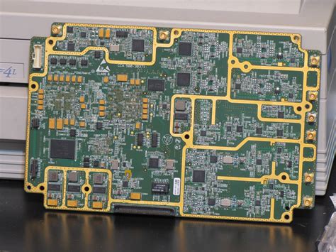
A Printed Circuit Board (PCB) is the backbone of modern electronics. It is a flat board made of insulating material, such as fiberglass or plastic, with conductive copper tracks printed on it to connect various electronic components. PCBs provide mechanical support and electrical connectivity for electronic devices, ranging from simple single-layer boards for basic projects to complex multi-layer boards for advanced applications.
PCBs are essential because they allow for the miniaturization and automation of electronic circuits. By etching the conductive tracks onto a flat board, PCBs eliminate the need for complex wiring and make it possible to mass-produce electronic devices efficiently. This has revolutionized the electronics industry and made modern technology possible.
The Evolution of PCB Technology
PCB technology has come a long way since its inception in the early 20th century. The first PCBs were made by hand, with conductive tracks painted onto a substrate using stencils. This was a time-consuming and error-prone process that limited the complexity of the circuits that could be produced.
In the 1950s, the introduction of photoengraving techniques allowed for the mass production of PCBs. This involved using a photomask to selectively expose a photoresist layer on the copper-clad board, which was then etched away to create the conductive tracks. This process greatly improved the accuracy and consistency of PCB production.
In the 1960s, the introduction of multi-layer PCBs further expanded the capabilities of PCB technology. By stacking multiple layers of insulating material and conductive tracks, PCBs could be made with much higher component densities and more complex interconnections. This enabled the development of smaller, more powerful electronic devices.
Today, PCB technology continues to evolve with the introduction of new materials, manufacturing processes, and design tools. Some of the latest advancements include:
-
High-Density Interconnect (HDI) PCBs: These PCBs use microvias and fine-pitch traces to achieve higher component densities and smaller form factors.
-
Flexible PCBs: These PCBs are made from flexible materials that can bend and fold, allowing for more creative and compact designs.
-
Metal Core PCBs: These PCBs use a metal core instead of a traditional FR4 substrate, which provides better thermal management for high-power applications.
-
3D Printed PCBs: Advances in 3D printing technology are enabling the rapid prototyping of PCBs with complex geometries and embedded components.

The Importance of Blank PCBs
While most PCBs are designed and manufactured for specific applications, blank PCBs are an essential tool for electronics enthusiasts, students, and professionals. A blank PCB is a bare board without any components or conductive tracks. It serves as a starting point for creating custom circuits and prototypes.
Blank PCBs offer several advantages over pre-designed boards:
-
Flexibility: With a blank PCB, you have complete control over the layout and functionality of your circuit. You can add or remove components, change the size and shape of the board, and experiment with different design options.
-
Cost-effectiveness: Blank PCBs are generally cheaper than pre-designed boards, especially for small-scale production or one-off projects. You only pay for the materials and manufacturing costs, without any markup for design or intellectual property.
-
Educational value: Building circuits on blank PCBs is an excellent way to learn about electronics and PCB design. By starting from scratch, you gain a deeper understanding of how components interact and how circuits work.
-
Customization: Blank PCBs allow you to create circuits that are tailored to your specific needs and requirements. You can add unique features, optimize performance, and integrate with other systems as needed.

Choosing the Right Blank PCB
When selecting a blank PCB for your project, there are several factors to consider:
| Factor | Description |
|---|---|
| Material | The most common materials are FR4 (fiberglass), aluminum, and flexible substrates. Choose based on your application’s requirements for strength, thermal management, and flexibility. |
| Layers | Single-layer boards are the simplest and cheapest, but multi-layer boards offer more routing options and higher component densities. |
| Thickness | PCB Thickness is measured in ounces of copper per square foot. Common thicknesses range from 0.5 oz to 2 oz, with thicker boards providing better current-carrying capacity but being more difficult to etch. |
| Surface Finish | The surface finish protects the copper traces from oxidation and improves solderability. Common options include HASL (Hot Air Solder Leveling), ENIG (Electroless Nickel Immersion Gold), and OSP (Organic Solderability Preservative). |
| Size | PCB sizes are typically specified in inches or millimeters. Choose a size that accommodates all your components and leaves room for mounting holes and connectors. |

Designing Your PCB Layout
Once you have selected your blank PCB, the next step is to design your circuit layout. This involves placing components on the board and routing the conductive tracks to connect them. There are several tools and techniques to help with this process:
Schematic Capture
Before laying out your PCB, it’s a good idea to create a schematic diagram of your circuit. This is a graphical representation of the components and their connections, using standardized symbols and notations. Schematic capture software like KiCad or Eagle can help you create and verify your schematic.
PCB Layout Software
To actually design your PCB layout, you’ll need specialized software that can translate your schematic into a physical board design. Popular options include KiCad, Eagle, and Altium Designer. These tools allow you to place components, route tracks, and generate manufacturing files.
Design Rules and Guidelines
When designing your PCB layout, it’s important to follow best practices and design rules to ensure manufacturability and reliability. Some key guidelines include:
- Maintaining minimum trace widths and clearances
- Avoiding acute angles and sharp corners
- Providing adequate space for component placement and soldering
- Using ground planes and power planes for better signal integrity
- Following manufacturer’s recommendations for component footprints and pad sizes
Manual vs. Autorouting
PCB layout software often includes autorouting features that can automatically generate track routes based on your schematic and design rules. While autorouting can be a time-saver, it’s not always the best option for complex or high-speed designs. Manual routing allows for more control over the placement of critical traces and can often result in a more optimized layout.
Manufacturing Your PCB
Once your PCB layout is complete, the next step is to manufacture the actual board. There are several options for PCB fabrication, depending on your budget, timeline, and quality requirements.
In-House Fabrication
If you have access to a PCB fabrication lab or makerspace, you may be able to manufacture your PCB in-house. This typically involves the following steps:
- Printing your PCB layout onto a transparency film to create a photomask.
- Exposing a photoresist-coated blank PCB to UV light through the photomask.
- Developing the photoresist to remove the unexposed areas.
- Etching away the exposed copper using a chemical solution.
- Drilling holes for through-hole components and vias.
- Applying a surface finish to protect the copper traces.
In-house fabrication can be a great option for quick prototypes or low-volume production, but it requires specialized equipment and expertise.
PCB Fabrication Services
For most projects, it’s more practical to outsource PCB fabrication to a professional service. There are many online PCB fabrication houses that can produce high-quality boards at reasonable prices, such as OSH Park, JLCPCB, and PCBWay.
To use a PCB fabrication service, you’ll need to generate manufacturing files from your PCB layout software. These typically include:
- Gerber files: These are the industry-standard files that describe the copper layers, solder mask, and silkscreen of your PCB.
- Drill files: These specify the location and size of all the holes in your PCB.
- Bill of Materials (BOM): This is a list of all the components used in your design, including their quantities and specifications.
Once you’ve uploaded your manufacturing files and placed your order, the fabrication house will produce your PCBs and ship them to you. Turnaround times can vary from a few days to a few weeks, depending on the complexity of your design and the fabricator’s workload.
Assembling Your PCB
With your blank PCB fabricated, the final step is to assemble your components onto the board. This can be done by hand soldering or using automated assembly techniques.
Hand Soldering
For small-scale production or prototypes, hand soldering is the most common assembly method. This involves using a soldering iron to melt solder onto the component leads and PCB pads, creating a permanent electrical and mechanical connection.
To ensure good soldering results, it’s important to:
- Use the right soldering iron temperature and tip size for your components.
- Apply heat to both the component lead and PCB pad simultaneously.
- Use enough solder to create a good fillet, but not so much that it causes bridging or shorts.
- Inspect your solder joints for good wetting and consistency.
Automated Assembly
For larger-scale production or more complex designs, automated assembly techniques can be used. These include:
- Solder Paste Stenciling: A metal stencil is used to apply solder paste onto the PCB pads, which is then heated to reflow the solder and attach the components.
- Pick-and-Place Machines: Automated machines are used to pick up components from reels or trays and place them onto the PCB with high precision.
- Reflow Ovens: The assembled PCBs are passed through a reflow oven, which heats the board to melt the solder and create a permanent bond between the components and pads.
Automated assembly can be more expensive and time-consuming to set up, but it offers greater consistency and efficiency for high-volume production.
Conclusion
Blank PCBs are a versatile and essential tool for anyone working with electronics. By understanding the basics of PCB design, fabrication, and assembly, you can create custom circuits that are tailored to your specific needs and requirements.
Whether you’re a hobbyist looking to learn more about electronics or a professional designer working on a complex project, blank PCBs offer a blank canvas for creativity and innovation. With the latest advancements in PCB technology, the possibilities are endless.
FAQs
- What are the advantages of using a blank PCB over a pre-designed board?
A: Blank PCBs offer greater flexibility, cost-effectiveness, educational value, and customization compared to pre-designed boards. With a blank PCB, you have complete control over the layout and functionality of your circuit, and you can create designs that are tailored to your specific needs and requirements.
- What factors should I consider when choosing a blank PCB?
A: When selecting a blank PCB, you should consider the material, number of layers, thickness, surface finish, and size based on your application’s requirements. These factors will affect the strength, thermal management, routing options, solderability, and component compatibility of your PCB.
- What tools do I need to design my own PCB layout?
A: To design your own PCB layout, you’ll need schematic capture software to create a schematic diagram of your circuit, and PCB layout software to translate your schematic into a physical board design. Popular options include KiCad, Eagle, and Altium Designer.
- Can I manufacture my own PCBs at home?
A: Yes, it is possible to manufacture PCBs at home or in a makerspace using specialized equipment and chemicals. The process typically involves creating a photomask, exposing and developing a photoresist-coated blank PCB, etching away the exposed copper, drilling holes, and applying a surface finish.
- What are the advantages of using a professional PCB fabrication service?
A: Professional PCB fabrication services offer several advantages over in-house fabrication, including higher quality, faster turnaround times, and the ability to handle more complex designs. They also have the equipment and expertise to produce PCBs with tighter tolerances and more advanced features, such as multi-layer boards, HDI, and specialized materials.
No responses yet