Introduction to PCB Pad Sizing
Properly sizing the pads on a printed circuit board (PCB) is critical for ensuring reliable solder joints and good electrical and mechanical connections between components and the board. PCB pad size calculations need to take into account factors like the component package dimensions, solder joint strength requirements, assembly processes, and PCB manufacturing capabilities and tolerances.
Incorrectly sized pads can lead to issues like poor solder wetting, weak solder joints, tombstoning of small chip components, and difficulties in assembly and rework. Therefore, it’s important for PCB designers to understand the best methods and guidelines for calculating optimal pad sizes.
Component Package Dimensions and Tolerances
The starting point for PCB pad size calculations is the dimensions of the component package that will be soldered to the pads. Most component manufacturers provide package drawings with detailed mechanical dimensions and tolerances.
Some key component package dimensions to consider include:
– Lead or termination width and thickness
– Pitch (spacing) between leads or terminations
– Overall package length and width
– Height of the package above the PCB
It’s important to use the maximum material condition (MMC) dimensions, which represent the largest size the features can be within the allowable tolerances. This ensures the pads will be sized to accommodate the worst-case component dimensions.
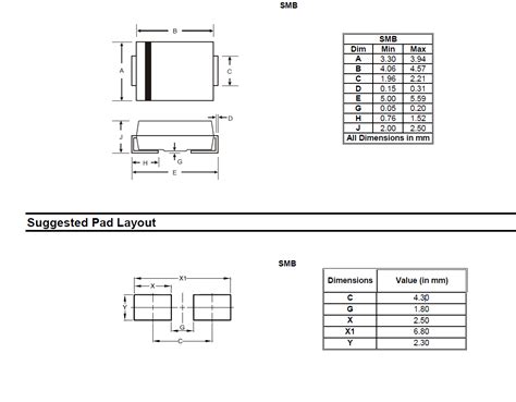
For example, consider a small outline integrated circuit (SOIC) package with the following dimensions and tolerances:
| Dimension | Nominal (mm) | Tolerance (mm) | MMC (mm) |
|---|---|---|---|
| Lead width | 0.40 | ±0.10 | 0.50 |
| Lead thickness | 0.15 | ±0.05 | 0.20 |
| Pitch | 1.27 | ±0.10 | 1.37 |
| Overall length | 5.00 | ±0.20 | 5.20 |
| Overall width | 3.90 | ±0.20 | 4.10 |
In this case, the pad size calculations would use the MMC lead width of 0.50 mm and the MMC pitch of 1.37 mm.
PCB Fabrication Capabilities and Tolerances
The capabilities and tolerances of the PCB fabrication process also play a role in pad size calculations. Most PCB manufacturers specify their minimum pad size and spacing requirements, as well as the tolerances on the pad dimensions.
Some typical PCB fabrication capabilities for pad sizes include:
| Capability | Minimum (mm) | Tolerance (mm) |
|---|---|---|
| Pad width | 0.20 | ±0.05 |
| Pad spacing | 0.20 | ±0.05 |
| Hole diameter | 0.30 | ±0.08 |
| Hole-to-pad spacing | 0.25 | ±0.05 |
It’s important to ensure the calculated pad dimensions are within the capabilities of the PCB fabricator and to account for the tolerances in the calculations. Overly small or tightly spaced pads may be difficult or impossible to manufacture reliably.

IPC Standards for Land Pattern Design
The IPC (formerly the Institute for Interconnecting and Packaging Electronic Circuits) publishes several standards that provide guidelines and requirements for PCB land pattern design, including pad sizing. The most relevant standards are:
- IPC-7351: Generic Requirements for Surface Mount Design and Land Pattern Standard
- IPC-SM-782: Surface Mount Design and Land Pattern Standard
- IPC-2221: Generic Standard on Printed Board Design
These standards provide formulas and tables for calculating pad sizes based on component dimensions and tolerances, solder joint requirements, and PCB fabrication capabilities. They are widely used in the electronics industry as a basis for PCB land pattern design.

Solder Joint Strength and Reliability
The strength and reliability of the solder joints between the component leads and PCB pads are critical for the overall reliability of the assembly. Solder joint strength is influenced by factors like the size and shape of the pads, the solder alloy used, and the soldering process parameters.
In general, larger pads with more solder fillet area will result in stronger solder joints. However, excessively large pads can cause issues like solder bridging or reduced space for routing traces between pads.
IPC-7351 provides guidelines for minimum and maximum solder fillet areas based on the component lead dimensions and the desired solder joint strength. For example, for a gullwing lead with a width of 0.50 mm and a thickness of 0.20 mm, the standard recommends a minimum fillet area of 0.60 mm² and a maximum fillet area of 1.20 mm².
Solder Paste Stencil Design
For surface mount assembly using solder paste, the size and shape of the openings in the solder paste stencil also need to be considered in pad size calculations. The stencil openings should be slightly smaller than the pad sizes to allow for some paste spread during reflow soldering.
A common guideline is to subtract a “pullback” or “shrinkage” factor from the pad dimensions to calculate the stencil opening dimensions. The pullback factor depends on the solder paste properties and the desired paste volume, but a typical value is around 0.05 mm.
For example, if the calculated pad size for a component lead is 0.60 mm x 1.00 mm, the corresponding stencil opening size would be 0.55 mm x 0.95 mm, using a pullback factor of 0.05 mm.
Thermal Pad Design for High-Power Components
For high-power surface mount components like transistors, voltage regulators, or power LEDs, the thermal pad design is critical for efficient heat transfer from the component to the PCB. The thermal pad is typically a large pad underneath the component package that conducts heat to the PCB’s ground or power planes.
The size of the thermal pad depends on the component’s power dissipation, the maximum allowable temperature rise, and the thermal conductivity of the PCB materials. Some general guidelines for thermal pad sizing include:
- The thermal pad area should be at least 4-5 times the area of the component package.
- The thermal pad should extend beyond the component package on all sides by at least 1-2 mm.
- Thermal vias should be used to conduct heat through the PCB to the opposite side or inner layers.
For example, for a surface mount voltage regulator in a TO-263 package with a power dissipation of 2 W and a maximum allowable temperature rise of 50°C, a thermal pad size of at least 6 mm x 6 mm with an array of thermal vias would be appropriate.
Pad Shape and Solder Mask Design
The shape of the pads and the solder mask openings around them can also affect the soldering process and joint reliability. Some common pad shapes include:
- Rectangular pads: Simple and widely used, but can be prone to tombstoning of small chip components.
- Rounded rectangular pads: Reduces stress concentrations and improves solder joint fillets, but may require more space.
- Teardrop pads: Used for through-hole components to strengthen the transition between the pad and the connecting trace.
Solder mask openings should be slightly larger than the pads to allow for solder wetting and fillets. A common guideline is to add a solder mask expansion of 0.05-0.10 mm around the pad edges.
PCB Assembly Process Considerations
The choice of PCB assembly process, such as wave soldering, reflow soldering, or hand soldering, can also influence pad size calculations. Different processes have different requirements for pad sizes, shapes, and spacings.
For example, wave soldering typically requires larger pads and spacings to accommodate the turbulent solder wave and prevent bridging. Reflow soldering allows for smaller pads and tighter spacings, but requires careful control of solder paste volume and placement.
Hand soldering can accommodate a wide range of pad sizes and shapes, but requires operator skill and can be time-consuming for large numbers of components.
It’s important to consider the intended assembly process during PCB design and pad size calculations, and to consult with the assembly provider for their specific requirements and guidelines.
Conclusion
Calculating optimal pad sizes for PCB design involves considering multiple factors, including component package dimensions, PCB fabrication capabilities, solder joint strength and reliability, assembly processes, and thermal management requirements.
Following industry standards like IPC-7351 and guidelines for solder mask design, stencil aperture sizing, and thermal pad design can help ensure robust and manufacturable PCB layouts.
Ultimately, the goal of pad size calculation is to achieve reliable and cost-effective PCB assemblies that meet the functional and environmental requirements of the end application.
FAQ
What are the most important factors to consider when calculating PCB pad sizes?
The most important factors are the component package dimensions and tolerances, the PCB fabrication capabilities and tolerances, the desired solder joint strength and reliability, and the intended assembly process.
How do I find the component package dimensions for pad size calculations?
Most component manufacturers provide detailed package drawings with mechanical dimensions and tolerances. Use the maximum material condition (MMC) dimensions that represent the largest size the features can be within the allowable tolerances.
What are some common PCB fabrication capabilities for pad sizes?
Typical capabilities include a minimum pad width and spacing of 0.20 mm with a tolerance of ±0.05 mm, a minimum hole diameter of 0.30 mm with a tolerance of ±0.08 mm, and a minimum hole-to-pad spacing of 0.25 mm with a tolerance of ±0.05 mm.
What industry standards provide guidelines for PCB pad sizing?
The most relevant IPC standards are IPC-7351 for generic surface mount design and land pattern requirements, IPC-SM-782 for surface mount design and land pattern standards, and IPC-2221 for generic printed board design.
How do I calculate the stencil aperture size for solder paste printing?
A common guideline is to subtract a “pullback” or “shrinkage” factor, typically around 0.05 mm, from the pad dimensions to calculate the stencil opening dimensions. This allows for some paste spread during reflow soldering.
No responses yet