Introduction to PCB Soldering
PCB (Printed Circuit Board) soldering is a crucial process in the manufacturing of electronic devices. It involves joining electronic components to the PCB using solder, a metal alloy that melts at a relatively low temperature. Proper PCB soldering ensures reliable electrical connections and the overall functionality of the device.
Types of PCB Soldering
There are two main types of PCB soldering:
- Through-hole soldering
- Components have long leads that are inserted through holes in the PCB
- Solder is applied to the leads on the opposite side of the board
-
Suitable for larger components and projects requiring high mechanical strength
-
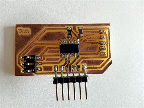
Surface mount soldering (SMD)
- Components have small leads or pads that are soldered directly onto the surface of the PCB
- Requires precise placement and soldering techniques
- Allows for smaller components and higher component density on the board
Challenges of Double-Sided PCB Soldering with SMD Parts
Double-sided PCB soldering with SMD parts presents unique challenges compared to single-sided or through-hole soldering:
- Alignment: Ensuring proper alignment of components on both sides of the board can be difficult.
- Heat management: Applying heat evenly to both sides of the board without damaging components requires careful temperature control.
- Solder bridging: The close proximity of SMD pads increases the risk of solder bridging, causing short circuits.
- Inspection: Visually inspecting soldered joints on both sides of the board can be challenging.
Best Design Practices for Double-Sided PCB Soldering with SMD Parts
To overcome these challenges and achieve reliable double-sided PCB soldering with SMD parts, follow these best design practices:
1. Component Placement
- Place components strategically to minimize interference between the top and bottom sides of the board.
- Avoid placing large components directly opposite each other on both sides of the board.
- Consider the placement of vias and through-hole components to prevent obstruction during soldering.
2. Pad Design
- Ensure SMD pads are appropriately sized for the component leads.
- Maintain proper spacing between pads to minimize the risk of solder bridging.
- Use solder mask to cover areas where solder is not desired, reducing the likelihood of short circuits.
3. Solder Paste Stencil Design
- Create a precise solder paste stencil to apply the correct amount of solder paste to the pads.
- Optimize the stencil aperture size and shape for each component type.
- Consider using step stencils for components with different heights to ensure even solder paste application.
4. Reflow Soldering Profile
- Develop a reflow soldering profile that gradually heats the board and components to the appropriate temperature.
- Ensure the peak temperature is high enough to melt the solder but not so high as to damage the components.
- Allow sufficient time for the solder to flow and form reliable joints.
5. Selective Soldering
- Use selective soldering techniques, such as a hot air pencil or soldering iron, for rework or touch-ups.
- Apply heat precisely to the desired area to avoid affecting nearby components.
- Use flux to improve solder flow and joint quality during selective soldering.
6. Inspection and Quality Control
- Implement a thorough visual inspection process to identify any soldering defects, such as bridging, insufficient solder, or poor joint formation.
- Use magnification tools or automated optical inspection (AOI) systems for more detailed examinations.
- Perform electrical tests to verify the functionality of the soldered components and the overall board.

Soldering Techniques for Double-Sided PCBs with SMD Parts
In addition to the best design practices, employing the right soldering techniques is essential for successful double-sided PCB soldering with SMD parts:
1. Solder Paste Application
- Use a solder paste stencil to apply solder paste evenly to the pads on both sides of the board.
- Ensure the stencil is properly aligned with the pads and has the correct thickness.
- Inspect the solder paste application for consistency and accuracy.
2. Component Placement
- Use a pick-and-place machine or manual placement tools to accurately position SMD components on the pads.
- Ensure the components are oriented correctly and aligned with the pads.
- Apply gentle pressure to maintain component positioning during the soldering process.
3. Reflow Soldering
- Place the populated PCB in a reflow oven or use a hot plate for smaller boards.
- Follow the predetermined reflow soldering profile to gradually heat the board and melt the solder.
- Monitor the temperature throughout the process to avoid overheating or underheating.
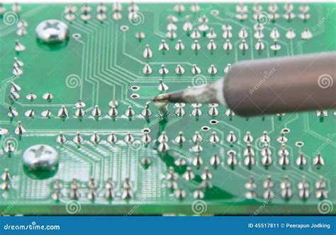
4. Selective Soldering
- For components that cannot withstand the reflow process or require rework, use selective soldering techniques.
- Apply heat directly to the component leads or pads using a hot air pencil or soldering iron.
- Use flux to improve solder flow and create a reliable joint.
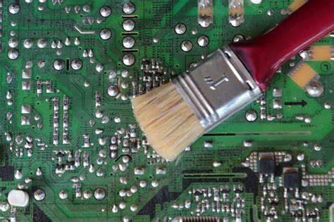
5. Cleaning and Inspection
- After soldering, clean the board to remove any flux residue or debris.
- Visually inspect the soldered joints for defects, such as bridging, insufficient solder, or poor wetting.
- Use magnification tools or automated inspection systems for more detailed analysis.
- Perform electrical tests to confirm the functionality of the soldered components and the overall board.
Common Soldering Defects and How to Prevent Them
Despite following best design practices and soldering techniques, defects can still occur. Here are some common soldering defects and ways to prevent them:
| Defect | Description | Prevention |
|---|---|---|
| Bridging | Solder accidentally connecting adjacent pads | – Maintain proper pad spacing – Use solder mask – Control solder paste volume |
| Insufficient Solder | Solder joint lacks enough solder to form a reliable connection | – Ensure adequate solder paste application – Optimize reflow soldering profile – Verify stencil aperture size |
| Poor Wetting | Solder fails to adhere to the pad or component lead | – Ensure pad and lead cleanliness – Use appropriate flux – Control soldering temperature |
| Tombstoning | Component stands up on one end due to uneven heating or pad design | – Balance pad sizes on both ends of the component – Optimize reflow soldering profile – Ensure even solder paste application |
Frequently Asked Questions (FAQ)
-
Q: What is the difference between through-hole and surface mount soldering?
A: Through-hole soldering involves inserting component leads through holes in the PCB and soldering on the opposite side, while surface mount soldering involves soldering components directly onto pads on the PCB surface. -
Q: Why is double-sided PCB soldering with SMD parts more challenging?
A: Double-sided PCB soldering with SMD parts is more challenging due to the need for proper alignment of components on both sides, even heat distribution, and the increased risk of solder bridging and defects. -
Q: How can I prevent solder bridging when soldering SMD components?
A: To prevent solder bridging, maintain proper pad spacing, use solder mask to cover areas where solder is not desired, and control the solder paste volume using a well-designed stencil. -
Q: What is a reflow soldering profile, and why is it important?
A: A reflow soldering profile is a predetermined temperature curve that gradually heats the PCB and components to the appropriate temperature for soldering. It is important because it ensures the solder melts and flows properly without damaging the components. -
Q: How can I inspect the quality of soldered joints on a double-sided PCB?
A: Visual inspection using magnification tools or automated optical inspection (AOI) systems can help identify soldering defects. Electrical tests can also be performed to verify the functionality of the soldered components and the overall board.
Conclusion
Double-sided PCB soldering with SMD parts requires careful planning, precise design, and appropriate soldering techniques to ensure reliable and functional electronic devices. By following best design practices, such as strategic component placement, proper pad design, and optimized reflow soldering profiles, you can minimize the risk of soldering defects and achieve high-quality results.
Additionally, employing the right soldering techniques, including accurate solder paste application, precise component placement, and selective soldering when necessary, further contributes to successful double-sided PCB soldering.
Regular inspection and quality control measures are essential to identify and address any soldering defects promptly. By understanding common defects and implementing preventive measures, you can optimize your double-sided PCB soldering process and produce reliable electronic devices.
As the electronics industry continues to advance, staying updated with the latest design practices, soldering techniques, and inspection methods will be crucial for anyone involved in PCB soldering. Continuous learning and adaptation will help you overcome the challenges of double-sided PCB soldering with SMD parts and deliver high-quality products consistently.
No responses yet