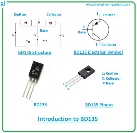
Introduction to Bd139 Transistor
The Bd139 is a popular NPN transistor widely used in various electronic applications. It is known for its high current gain, low saturation voltage, and excellent switching characteristics. Understanding the Bd139 Pinout is crucial for effectively utilizing this transistor in your projects.
Bd139 Pinout Configuration
The Bd139 transistor has three pins: the collector (C), base (B), and emitter (E). The pinout configuration is as follows:
| Pin | Symbol | Description |
|---|---|---|
| 1 | E | Emitter |
| 2 | B | Base |
| 3 | C | Collector |
It’s essential to identify the correct pinout when connecting the Bd139 in a circuit to ensure proper functionality and avoid damage to the transistor or other components.
Package Types and Pinout Variations
The Bd139 transistor is available in different package types, such as TO-126, TO-220, and SOT-32. While the pinout remains the same across these packages, the physical layout and dimensions may vary. Always refer to the specific datasheet of the package you are using for accurate information.
Bd139 Electrical Characteristics
To effectively use the Bd139 transistor, it’s crucial to understand its electrical characteristics. Here are some key parameters:
Maximum Ratings
| Parameter | Symbol | Value |
|---|---|---|
| Collector-Emitter Voltage | VCEO | 80V |
| Collector-Base Voltage | VCBO | 100V |
| Emitter-Base Voltage | VEBO | 5V |
| Collector Current | IC | 1.5A |
| Total Power Dissipation | Ptot | 12.5W |
It’s important not to exceed these maximum ratings to prevent damage to the transistor.
Current Gain (hFE)
The current gain, or hFE, is a critical parameter that determines the amplification capability of the transistor. For the Bd139, the typical current gain ranges from 100 to 250, depending on the collector current and temperature.
Collector-Emitter Saturation Voltage (VCE(sat))
The collector-emitter saturation voltage, or VCE(sat), is the voltage drop across the transistor when it is fully saturated. For the Bd139, the typical VCE(sat) is around 0.5V at a collector current of 500mA.

Bd139 Applications
The Bd139 transistor finds applications in various circuits, including:
-
Switching Circuits: The Bd139 is commonly used as a switch in power control, motor control, and relay driving circuits.
-
Amplifier Circuits: It can be employed in audio amplifiers, voltage amplifiers, and current amplifiers.
-
Voltage Regulators: The Bd139 is suitable for use in voltage regulator circuits, providing stable and regulated output voltages.
-
Driver Circuits: It is often used as a driver transistor for high-current loads, such as LEDs, buzzers, and solenoids.
Bd139 Circuit Design Considerations
When designing circuits with the Bd139 transistor, consider the following:
Biasing
Proper biasing is essential to ensure the transistor operates in the desired region (active, saturation, or cut-off). The base-emitter voltage (VBE) and base current (IB) must be carefully selected based on the desired collector current (IC) and the transistor’s current gain (hFE).
Heat Dissipation
The Bd139 can dissipate a significant amount of power, especially when operating at high currents. Adequate heat sinking and thermal management are crucial to prevent overheating and ensure reliable operation.
Input and Output Impedance
Consider the input and output impedance of the circuit when using the Bd139. Proper impedance matching is necessary to maximize signal transfer and minimize distortion.
Bd139 Pinout Diagram and Schematic Symbol
Here’s a visual representation of the Bd139 pinout and its schematic symbol:
[Insert Bd139 pinout diagram and schematic symbol image]
Understanding the pinout and schematic symbol is essential for correctly integrating the Bd139 into your circuit designs.
Frequently Asked Questions (FAQ)
- What is the maximum collector current of the Bd139 transistor?
-
The maximum collector current (IC) of the Bd139 is 1.5A.
-
Can the Bd139 be used as a switch?
-
Yes, the Bd139 is commonly used as a switch in various power control and relay driving applications.
-
What is the typical current gain (hFE) of the Bd139?
-
The typical current gain (hFE) of the Bd139 ranges from 100 to 250, depending on the collector current and temperature.
-
Is heat sinking necessary when using the Bd139?
-
Yes, proper heat sinking is crucial when using the Bd139, especially at high currents, to prevent overheating and ensure reliable operation.
-
Can the Bd139 be used in audio amplifier circuits?
- Yes, the Bd139 is suitable for use in audio amplifier circuits, providing good amplification and low distortion.
Conclusion
The Bd139 transistor is a versatile and widely used NPN transistor known for its high current gain, low saturation voltage, and excellent switching characteristics. Understanding the Bd139 pinout and its electrical characteristics is essential for effectively utilizing this transistor in various electronic applications.
By considering factors such as biasing, heat dissipation, and impedance matching, you can design robust and efficient circuits using the Bd139. Whether you’re working on switching circuits, amplifiers, voltage regulators, or driver circuits, the Bd139 is a reliable choice.
Remember to always refer to the specific datasheet of the Bd139 package you are using for accurate information on pinout, dimensions, and electrical characteristics.
With this comprehensive technical guide, you now have the knowledge and understanding to confidently incorporate the Bd139 transistor into your electronic projects and unlock its full potential.

No responses yet