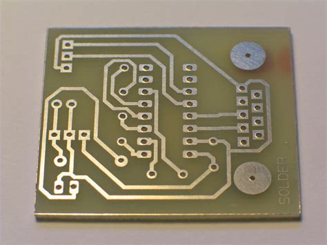
What is a Bare Printed Circuit Board (PCB)?
A bare printed circuit board, also known as a blank PCB, is a foundation for building electronic circuits. It is a flat board made of insulating material, typically fiberglass or composite epoxy, with conductive copper traces printed on one or both sides. These traces form the electrical connections between various components that will be soldered onto the board later in the manufacturing process.
Bare PCBs are essential in the world of electronics, as they provide a stable and organized platform for mounting and connecting electronic components. They are used in a wide range of applications, from simple hobby projects to complex industrial equipment and consumer electronics.
Key Features of a Bare PCB
- Substrate material: The base material of the PCB, which is usually fiberglass or composite epoxy.
- Copper layers: The number of conductive copper layers on the board, which can range from one to multiple layers.
- Thickness: The thickness of the PCB, which is typically measured in millimeters or mils (thousandths of an inch).
- Copper weight: The amount of copper used in the conductive layers, usually measured in ounces per square foot.
- Solder mask: A protective coating applied to the PCB to prevent short circuits and improve solderability.
- Silkscreen: A printed layer on the PCB that provides labels, logos, and other identifying information.
Types of Bare PCBs
There are several types of bare PCBs, each with its own unique characteristics and applications. The most common types include:
1. Single-Sided PCBs
Single-sided PCBs have conductive copper traces on only one side of the board. They are the simplest and most cost-effective type of PCB, making them ideal for low-complexity projects and prototypes.
2. Double-Sided PCBs
Double-sided PCBs have conductive copper traces on both sides of the board, allowing for more complex circuit designs and higher component density. The two sides are connected using plated through-holes (PTHs) or vias.
3. Multi-Layer PCBs
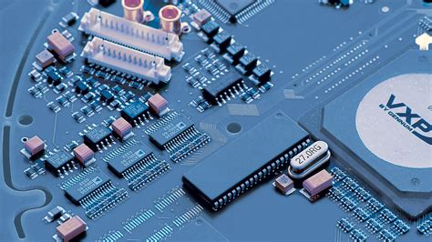
Multi-layer PCBs consist of three or more conductive layers separated by insulating layers. They offer the highest level of complexity and density, enabling the creation of intricate circuits with a smaller footprint. Multi-layer PCBs are commonly used in advanced electronics, such as smartphones, computers, and aerospace applications.
4. Flexible PCBs
Flexible PCBs are made of thin, flexible materials that allow the board to bend and conform to various shapes. They are often used in wearable devices, medical equipment, and applications where space is limited or where the board needs to fit into a non-planar form factor.
5. Rigid-Flex PCBs
Rigid-flex PCBs combine the benefits of both rigid and flexible PCBs. They consist of rigid sections connected by flexible sections, enabling the board to be folded or bent in specific areas while maintaining stability in others. Rigid-flex PCBs are frequently used in aerospace, military, and automotive applications.
PCB Materials
The choice of materials used in a bare PCB can significantly impact its performance, durability, and cost. The most common materials used for PCB substrates and conductors are:
1. Substrate Materials
- FR-4: A composite material made of fiberglass and epoxy resin, FR-4 is the most widely used substrate material for PCBs due to its good electrical insulation properties, mechanical strength, and affordability.
- High-Frequency Materials: For applications requiring high-frequency operation, such as RF and microwave circuits, specialized substrate materials like Rogers, Teflon, and ceramic-based laminates are used to minimize signal loss and maintain signal integrity.
- Polyimide: A flexible, heat-resistant material used in flexible PCBs and applications that require high temperature tolerance.
2. Conductor Materials
- Copper: The most common conductor material used in PCBs, copper offers excellent electrical conductivity, thermal conductivity, and solderability.
- Gold: Sometimes used as a finish for high-reliability applications or as a contact material for connectors and switches.
- Silver: Occasionally used as a conductive ink for Printed Electronics or as a finish for high-frequency applications.

PCB Manufacturing Process
The manufacturing process for bare PCBs involves several steps, each of which contributes to the overall quality and functionality of the final board. The main steps in the PCB manufacturing process are:
- Design and Layout: The circuit schematic is created, and the physical layout of the components and traces is designed using PCB design software.
- Substrate Preparation: The substrate material is cut to the desired size and shape, and any necessary holes are drilled.
- Copper Deposition: A thin layer of copper is deposited onto the substrate using techniques like electroless plating or electrodeposition.
- Patterning: The desired circuit pattern is transferred onto the copper layer using photolithography or silk-screening techniques.
- Etching: The unwanted copper is removed using a chemical etching process, leaving only the desired circuit traces.
- Lamination (for multi-layer PCBs): The individual layers are aligned and bonded together under heat and pressure to form a multi-layer board.
- Drilling: Holes are drilled through the board to accommodate through-hole components and vias.
- Plating: The drilled holes are plated with copper to create electrical connections between layers.
- Solder Mask Application: A protective solder mask is applied to the board to prevent short circuits and improve solderability.
- Silkscreen Printing: Labels, logos, and other identifying information are printed onto the board using silkscreen printing.
- Surface Finish: A final surface finish, such as HASL (Hot Air Solder Leveling), ENIG (Electroless Nickel Immersion Gold), or OSP (Organic Solderability Preservative), is applied to protect the copper traces and enhance solderability.
- Quality Control: The finished bare PCB undergoes rigorous quality control tests to ensure it meets the required specifications and standards.
PCB Design Considerations
When designing a bare PCB, several factors must be considered to ensure optimal performance, reliability, and manufacturability. Some key design considerations include:
- Component Placement: Components should be placed in a logical and efficient manner, taking into account factors such as signal integrity, heat dissipation, and ease of assembly.
- Trace Width and Spacing: The width and spacing of the copper traces should be carefully designed to minimize signal interference, ensure proper current carrying capacity, and comply with manufacturing capabilities.
- Via Placement and Size: Vias should be strategically placed to minimize signal reflections and losses, and their size should be appropriate for the desired current carrying capacity and manufacturing process.
- Grounding and Shielding: Proper grounding and shielding techniques should be employed to minimize electromagnetic interference (EMI) and ensure signal integrity.
- Thermal Management: The PCB layout should be designed to facilitate heat dissipation from components, using techniques such as copper pours, thermal vias, and appropriate component placement.
- Manufacturing Constraints: The design must adhere to the capabilities and limitations of the chosen manufacturing process, such as minimum trace width, minimum drill size, and clearance requirements.
PCB testing and Inspection
To ensure the quality and reliability of bare PCBs, various testing and inspection methods are employed throughout the manufacturing process and after production. Some common testing and inspection techniques include:
- Visual Inspection: A manual or automated visual inspection of the PCB to identify any surface defects, such as scratches, contamination, or incomplete copper etching.
- Automated Optical Inspection (AOI): An automated system that uses cameras and image processing software to detect surface defects and verify the correctness of the PCB layout.
- Electrical Testing: Various electrical tests, such as continuity testing, insulation resistance testing, and high-potential (hipot) testing, are performed to ensure the electrical integrity of the board and to detect any short circuits or open connections.
- Microsectioning: A destructive testing method where a small cross-section of the PCB is removed and examined under a microscope to assess the quality of plated through-holes, vias, and lamination.
- X-ray Inspection: Non-destructive testing using X-ray imaging to inspect the internal structure of the PCB, particularly for multi-layer boards and to detect any voids or delamination.
- Functional Testing: The bare PCB is populated with components and tested under real-world operating conditions to verify its functionality and performance.
PCB standards and Certifications
To ensure consistency, reliability, and safety in the PCB industry, various standards and certifications have been established by international organizations and regulatory bodies. Some key standards and certifications include:
- IPC Standards: The Association Connecting Electronics Industries (IPC) publishes a wide range of standards for PCB design, manufacturing, and testing, such as IPC-A-600 (Acceptability of Printed Boards), IPC-6012 (Qualification and Performance Specification for Rigid Printed Boards), and IPC-2221 (Generic Standard on Printed Board Design).
- UL Certification: Underwriters Laboratories (UL) offers certification for PCBs used in safety-critical applications, ensuring they meet strict safety requirements and are suitable for use in specific environments.
- RoHS Compliance: The Restriction of Hazardous Substances (RoHS) directive restricts the use of certain hazardous materials in electronic products, including PCBs. RoHS-compliant PCBs are free from lead, mercury, cadmium, and other restricted substances.
- ISO Standards: The International Organization for Standardization (ISO) publishes standards related to PCB manufacturing and quality management, such as ISO 9001 (Quality Management Systems) and ISO 14001 (Environmental Management Systems).
Choosing a PCB Manufacturer
Selecting the right PCB manufacturer is crucial for ensuring the quality, reliability, and timely delivery of your bare PCBs. When choosing a PCB manufacturer, consider the following factors:
- Capabilities: Ensure the manufacturer has the necessary equipment, expertise, and experience to produce PCBs that meet your specific requirements, such as layer count, material selection, and surface finish options.
- Quality Control: Look for a manufacturer with a robust quality control system, preferably one that adheres to recognized industry standards and certifications, such as IPC and ISO.
- Turnaround Time: Consider the manufacturer’s typical turnaround times and their ability to accommodate your production schedule, particularly for time-sensitive projects.
- Cost: Obtain quotes from multiple manufacturers and compare their pricing, taking into account factors such as minimum order quantities, setup fees, and shipping costs.
- Customer Support: Choose a manufacturer with responsive and knowledgeable customer support, as this can be invaluable when addressing technical questions, design issues, or production concerns.
- Reputation and Reviews: Research the manufacturer’s reputation in the industry and read reviews from previous customers to gauge their level of service, quality, and reliability.
Frequently Asked Questions (FAQ)
- What is the difference between a bare PCB and an assembled PCB?
-
A bare PCB is a printed circuit board without any components soldered onto it, while an assembled PCB has all the necessary components mounted and soldered in place, ready for use in an electronic device.
-
Can I design my own PCB?
-
Yes, you can design your own PCB using various PCB design software tools, such as Altium Designer, Eagle, or KiCad. However, it is essential to have a good understanding of PCB design principles and to adhere to the manufacturing capabilities of your chosen PCB manufacturer.
-
What is the typical turnaround time for bare PCB production?
-
The turnaround time for bare PCB production can vary depending on the complexity of the design, the chosen manufacturer, and the current market conditions. Typically, turnaround times range from a few days to several weeks, with expedited options available at an additional cost.
-
How much does it cost to manufacture a bare PCB?
-
The cost of manufacturing a bare PCB depends on several factors, such as the board size, layer count, material selection, surface finish, and order quantity. Generally, prices range from a few dollars to several hundred dollars per board, with lower per-unit costs for larger order quantities.
-
What is the minimum order quantity (MOQ) for bare PCBs?
- The minimum order quantity for bare PCBs varies among manufacturers and depends on the specific requirements of the PCB design. Some manufacturers offer low MOQs for prototype and small-batch production, while others may require higher MOQs for more complex designs or to achieve cost-effective production.
Conclusion
Bare printed circuit boards are the foundation of modern electronics, providing a reliable and efficient means of connecting and organizing electronic components. Understanding the types, materials, manufacturing processes, and design considerations involved in bare PCB production is essential for anyone working in the electronics industry or embarking on an electronic project.
By selecting the right PCB manufacturer, adhering to industry standards and best practices, and thoroughly testing and inspecting the finished boards, you can ensure the quality, reliability, and performance of your electronic devices. As technology continues to advance, the role of bare PCBs in enabling innovative and compact electronic solutions will only become more crucial, making a deep understanding of these essential components all the more valuable.
No responses yet