Introduction to Bare PCBs
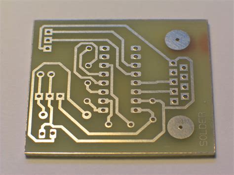
A bare printed circuit board (PCB) is the foundation of every electronic device we use today. It is a flat, insulating board made of fiberglass, composite epoxy, or other laminate material, with conductive copper traces printed on one or both sides. These copper traces connect various electronic components, such as resistors, capacitors, and integrated circuits (ICs), to create a functional electronic circuit.
Bare PCBs, also known as blank boards, are the starting point for any electronic design. They provide a platform for engineers and hobbyists to create custom circuits for their projects. Understanding the basics of bare PCBs is essential for anyone interested in electronics manufacturing or PCB assembly.
Types of Bare PCBs
There are several types of bare PCBs, each with its own unique characteristics and applications. The most common types include:
Single-Sided PCBs
Single-sided PCBs have copper traces on only one side of the board. They are the simplest and most cost-effective type of PCB, making them ideal for simple, low-density circuits. Single-sided PCBs are commonly used in consumer electronics, such as toys, calculators, and remote controls.
Double-Sided PCBs
Double-sided PCBs have copper traces on both sides of the board, allowing for more complex circuit designs and higher component density. The two sides are connected using through-hole vias, which are small holes drilled through the board and plated with conductive material. Double-sided PCBs are used in a wide range of applications, from automotive electronics to industrial control systems.
Multi-Layer PCBs
Multi-layer PCBs consist of three or more layers of copper traces, separated by insulating layers. They offer the highest component density and most complex circuit designs, making them ideal for advanced applications such as smartphones, computers, and medical devices. Multi-layer PCBs can have up to 50 layers, depending on the complexity of the circuit.
Flexible PCBs
Flexible PCBs, or flex circuits, are made from thin, flexible materials such as polyimide or polyester. They can bend and fold to fit into tight spaces or conform to irregular shapes, making them ideal for wearable electronics, aerospace applications, and medical devices. Flexible PCBs can be single-sided, double-sided, or multi-layer, depending on the application requirements.
Rigid-Flex PCBs
Rigid-flex PCBs combine the benefits of both rigid and flexible PCBs. They consist of rigid PCB sections connected by flexible PCB sections, allowing for 3D circuit designs and improved reliability in applications that require both stability and flexibility, such as automotive electronics, aerospace systems, and industrial robotics.

PCB Materials
The choice of material for a bare PCB depends on the application requirements, such as temperature range, dielectric constant, and mechanical strength. The most common PCB materials include:
FR-4
FR-4 is the most widely used PCB material, consisting of a woven fiberglass cloth impregnated with an epoxy resin. It offers good mechanical strength, thermal stability, and electrical insulation properties, making it suitable for a wide range of applications.
High-Frequency Materials
For high-frequency applications, such as RF and microwave circuits, special PCB materials with lower dielectric constants and loss tangents are used. These materials, such as Rogers laminates, PTFE, and ceramic-filled composites, help minimize signal loss and maintain signal integrity at higher frequencies.
Aluminum and Copper Core PCBs
Aluminum and copper core PCBs are used in applications that require enhanced thermal management, such as high-power LED lighting and motor control systems. The metal core helps dissipate heat more efficiently, improving the overall performance and reliability of the circuit.

PCB Manufacturing Process
The manufacturing process for bare PCBs involves several steps, each critical to ensuring the quality and reliability of the final product. The main steps include:
-
Design and Layout: The PCB design is created using electronic design automation (EDA) software, such as Altium Designer or KiCad. The layout defines the placement of components, routing of copper traces, and the overall board dimensions.
-
Printing: The PCB layout is printed onto a transparent film or photomask, which will be used to transfer the circuit pattern onto the copper-clad laminate.
-
Etching: The copper-clad laminate is coated with a light-sensitive photoresist and exposed to UV light through the photomask. The unexposed areas of the photoresist are then removed, leaving the desired circuit pattern. The exposed copper is etched away using a chemical solution, while the copper protected by the photoresist remains intact.
-
Drilling: Holes are drilled through the board to accommodate through-hole components and vias. The drilling process is typically automated using CNC machines.
-
Plating: For double-sided and multi-layer PCBs, the drilled holes are plated with a conductive material, such as copper, to create electrical connections between the layers.
-
Solder Mask and Silkscreen: A solder mask, typically green in color, is applied to the PCB to protect the copper traces from oxidation and prevent accidental short circuits during soldering. A silkscreen layer is then added to provide text and symbols for component placement and identification.
-
Surface Finish: A surface finish, such as HASL (Hot Air Solder Leveling), ENIG (Electroless Nickel Immersion Gold), or OSP (Organic Solderability Preservative), is applied to the exposed copper to enhance solderability and protect the copper from oxidation.
-
Electrical Testing: The completed bare PCB undergoes electrical testing to ensure that all connections are correct and there are no short circuits or open circuits.

PCB Design Considerations
When designing a bare PCB, several factors must be considered to ensure optimal performance, reliability, and manufacturability:
Signal Integrity
Maintain signal integrity by minimizing crosstalk, reflections, and electromagnetic interference (EMI). This can be achieved through proper trace routing, impedance matching, and the use of ground planes and shielding.
Power Integrity
Ensure stable and clean power delivery to all components by using appropriate decoupling capacitors, power planes, and proper power distribution networks (PDNs).
Thermal Management
Consider the thermal requirements of your components and design the PCB to efficiently dissipate heat. This may involve the use of thermal vias, metal core PCBs, or external heatsinks.
Manufacturability
Design your PCB with manufacturability in mind, adhering to the capabilities and limitations of your chosen PCB manufacturer. This includes minimum trace widths and spacings, hole sizes, and component clearances.
PCB Assembly
Once the bare PCB is manufactured, it undergoes the assembly process to populate it with electronic components. The two main PCB assembly methods are:
Through-Hole Assembly (THA)
Through-hole components have long leads that are inserted into holes drilled through the PCB and soldered onto the opposite side. THA is generally used for larger, more robust components and is well-suited for applications that require high mechanical strength or manual assembly.
Surface Mount Assembly (SMA)
Surface mount components are smaller and have flat leads or terminations that are soldered directly onto the surface of the PCB. SMA allows for higher component density, improved performance, and automated assembly using pick-and-place machines. Most modern electronic devices use surface mount technology (SMT) for the majority of their components.
Bare PCB Testing and Inspection
To ensure the quality and reliability of bare PCBs, various testing and inspection methods are employed during and after the manufacturing process:
Automated Optical Inspection (AOI)
AOI systems use high-resolution cameras and image processing algorithms to inspect the PCB for defects such as missing or misaligned components, solder bridges, and incorrect component polarity.
X-Ray Inspection
X-ray inspection is used to detect hidden defects, such as voids in solder joints or internal failures in multi-layer PCBs.
In-Circuit Testing (ICT)
ICT involves using a bed-of-nails fixture to make electrical contact with specific points on the PCB and test for shorts, opens, and component functionality.
Functional Testing
Functional testing verifies that the assembled PCB performs as intended in its final application, ensuring that all components and subsystems work together correctly.
Frequently Asked Questions (FAQ)
-
What is the difference between a bare PCB and an assembled PCB?
A bare PCB is a blank board with copper traces and no components, while an assembled PCB has electronic components soldered onto it, ready for use in an electronic device. -
Can I design my own PCB?
Yes, with the help of EDA software and some basic knowledge of electronics and PCB design principles, you can design your own PCB. Many online resources and tutorials are available to help you get started. -
How much does it cost to manufacture a bare PCB?
The cost of manufacturing a bare PCB depends on factors such as the board size, complexity, material, and quantity. Small, simple PCBs can cost as little as a few dollars each, while larger, more complex boards can cost several hundred dollars or more. -
What is the typical turnaround time for bare PCB manufacturing?
Turnaround times vary depending on the PCB manufacturer and the complexity of the board. Standard lead times range from a few days to several weeks, but expedited services are often available for an additional cost. -
Can I reuse a bare PCB for a different project?
In most cases, a bare PCB is designed for a specific circuit and cannot be easily reused for a different project. However, if the new project has similar requirements and the PCB layout is compatible, it may be possible to modify the existing design to suit the new application.
Conclusion
Bare printed circuit boards are the backbone of the electronics industry, providing a platform for engineers and hobbyists to create custom circuits for a wide range of applications. Understanding the types, materials, manufacturing processes, and design considerations of bare PCBs is essential for anyone involved in electronics design or manufacturing.
As technology advances, the demand for more complex, high-performance, and reliable PCBs will continue to grow. By staying up-to-date with the latest developments in PCB materials, manufacturing techniques, and design tools, engineers and manufacturers can create innovative electronic products that shape our future.
No responses yet