Introduction to BGA Packaging
Ball Grid Array (BGA) is a high-density surface mount package that has gained significant popularity in the electronics industry for packaging integrated circuits (ICs). BGA packages offer numerous advantages over traditional packaging techniques, such as smaller footprints, better electrical performance, and higher interconnect density. In this article, we will explore the fundamentals of BGA packaging, its benefits, manufacturing process, applications, and future trends.
What is a Ball Grid Array (BGA)?
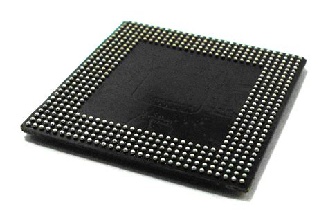
A Ball Grid Array (BGA) is a surface mount package that uses an array of solder balls as the interconnect between the IC and the printed circuit board (PCB). The solder balls are arranged in a grid pattern on the bottom side of the package, allowing for a high density of interconnects in a small area. BGA packages can have hundreds or even thousands of solder balls, depending on the size and complexity of the IC.
BGA Package Construction
A typical BGA package consists of the following components:
-
Substrate: The substrate is a thin, multi-layered laminate that provides mechanical support and electrical interconnection between the IC die and the solder balls. The substrate material is usually made of bismaleimide triazine (BT) or polyimide.
-
IC Die: The integrated circuit die is attached to the top side of the substrate using a die attach adhesive. Wire bonding or flip-chip technology is used to establish electrical connections between the die and the substrate.
-
Solder Balls: An array of solder balls is attached to the bottom side of the substrate. The solder balls are typically made of a lead-free solder alloy, such as tin-silver-copper (SAC).
-
Encapsulant: The IC die and wire bonds (if present) are protected by an encapsulant material, such as epoxy resin.
BGA Package Types
There are several types of BGA packages, each with its own unique features and applications:
-
Plastic BGA (PBGA): PBGA packages use a plastic substrate and are commonly used for low-cost, high-volume applications.
-
Ceramic BGA (CBGA): CBGA packages use a ceramic substrate and offer better thermal and electrical performance compared to PBGA packages. They are often used in high-reliability applications.
-
Tape BGA (TBGA): TBGA packages use a flexible tape substrate and are known for their thin profile and low weight. They are commonly used in mobile and portable devices.
-
Flip Chip BGA (FCBGA): FCBGA packages use flip-chip technology to attach the IC die directly to the substrate, eliminating the need for wire bonding. This results in better electrical performance and a smaller package size.

Advantages of BGA Packaging
BGA packages offer several advantages over traditional packaging techniques, such as quad flat packages (QFPs) and pin grid arrays (PGAs):
-
Smaller Footprint: BGA packages have a smaller footprint compared to QFPs and PGAs with the same number of interconnects. This allows for more compact PCB designs and higher component density.
-
Better Electrical Performance: The shorter interconnect lengths in BGA packages result in lower inductance and resistance, leading to better signal integrity and higher operating speeds.
-
Higher Interconnect Density: BGA packages can accommodate a large number of interconnects in a small area, making them suitable for complex ICs with high I/O counts.
-
Improved Thermal Performance: The grid array of solder balls provides a larger surface area for heat dissipation, resulting in better thermal performance compared to peripheral-leaded packages.
-
Enhanced Reliability: BGA packages offer better resistance to mechanical stress and thermal cycling, leading to improved reliability in demanding applications.

BGA Manufacturing Process
The manufacturing process for BGA packages involves several steps:
-
Substrate Fabrication: The multi-layered substrate is fabricated using a lamination process, with conductive traces and vias forming the electrical interconnections.
-
Die Attach: The IC die is attached to the substrate using a die attach adhesive, such as epoxy or solder.
-
Wire Bonding or Flip Chip Attach: Electrical connections between the die and the substrate are established using wire bonding or flip-chip technology.
-
Encapsulation: The IC die and wire bonds (if present) are encapsulated using an epoxy resin to protect them from mechanical damage and environmental factors.
-
Solder Ball Attach: An array of solder balls is attached to the bottom side of the substrate using a solder reflow process.
-
Singulation: The substrate panel is singulated into individual BGA packages using a sawing or punching process.
-
Testing and Inspection: The BGA packages undergo various tests and inspections to ensure quality and reliability.

Applications of BGA Packages
BGA packages are widely used in various electronic applications, including:
-
Mobile Devices: BGA packages are commonly used in smartphones, tablets, and wearable devices due to their small footprint and high interconnect density.
-
High-Performance Computing: BGA packages are used in microprocessors, graphics processing units (GPUs), and field-programmable gate arrays (FPGAs) for high-performance computing applications.
-
Networking and Telecommunications: BGA packages are employed in routers, switches, and other networking equipment for high-speed data transmission.
-
Automotive Electronics: BGA packages are used in advanced driver assistance systems (ADAS), infotainment systems, and other automotive electronic applications.
-
Industrial and Medical Electronics: BGA packages are used in industrial control systems, medical imaging devices, and other applications that require high reliability and performance.
Future Trends in BGA Packaging
As the demand for smaller, faster, and more complex electronic devices continues to grow, BGA packaging technology is evolving to meet these challenges:
-
3D Packaging: 3D BGA packages, such as package-on-package (PoP) and through-silicon via (TSV) technologies, are gaining traction for high-density integration and improved performance.
-
Embedded Devices: BGA packages are being used in embedded devices, such as system-on-chip (SoC) and system-in-package (SiP) solutions, for compact and highly integrated electronic systems.
-
Advanced Materials: New substrate materials, such as low-loss dielectrics and high-thermal conductivity materials, are being developed to improve the electrical and thermal performance of BGA packages.
-
Fine-pitch BGA: The pitch (distance) between solder balls is being reduced to accommodate higher interconnect density and smaller package sizes.
-
Environmental Sustainability: Lead-free solder alloys and halogen-free substrate materials are being adopted to minimize the environmental impact of BGA packages.
FAQ
-
Q: What is the difference between a BGA and a QFP package?
A: BGA packages have solder balls arranged in a grid array on the bottom side of the package, while QFP packages have leads extending from the periphery of the package. BGA packages offer a smaller footprint, higher interconnect density, and better electrical and thermal performance compared to QFP packages. -
Q: Can BGA packages be reworked or repaired?
A: Yes, BGA packages can be reworked or repaired using specialized equipment and techniques, such as hot air reflow and solder ball replacement. However, the process can be challenging and requires skilled technicians to avoid damaging the package or the PCB. -
Q: Are BGA packages more expensive than other packaging types?
A: BGA packages can be more expensive than traditional packaging types, such as QFPs and PGAs, due to the higher complexity of the substrate and the solder ball attach process. However, the cost difference has been decreasing over time as BGA packaging technology has matured and become more widely adopted. -
Q: How do I select the appropriate BGA package for my application?
A: When selecting a BGA package, consider factors such as the IC die size, I/O count, thermal requirements, electrical performance, reliability, and cost. Consult with the IC manufacturer or a packaging specialist to determine the most suitable BGA package type and configuration for your specific application. -
Q: What are the challenges associated with BGA packaging?
A: Some challenges associated with BGA packaging include the need for precise alignment during assembly, the difficulty in inspecting solder joint quality, the potential for thermal mismatch between the package and the PCB, and the complexity of rework and repair processes. Proper design, manufacturing, and testing practices can help mitigate these challenges.
Conclusion
Ball Grid Array (BGA) packaging has revolutionized the electronics industry by providing a high-density, high-performance, and compact solution for packaging integrated circuits. With its numerous advantages, including smaller footprints, better electrical and thermal performance, and higher interconnect density, BGA packages have become the preferred choice for a wide range of electronic applications.
As technology advances and the demand for more complex and miniaturized electronic devices grows, BGA packaging will continue to evolve, with new materials, technologies, and design innovations driving the future of IC packaging. By understanding the fundamentals of BGA packaging, its benefits, and its applications, engineers and designers can make informed decisions when selecting and designing BGA-based electronic systems.
No responses yet