Introduction to PCB Drilling
Printed Circuit Boards (PCBs) are essential components in modern electronic devices. The process of manufacturing PCBs involves several critical steps, one of which is drilling. PCB drilling is the process of creating holes in the PCB substrate to allow for the insertion of electronic components and the creation of interconnections between layers. Among the various drilling techniques used in PCB manufacturing, back drilling has gained significant importance due to its ability to enhance signal integrity and reduce signal distortion.
What is Back Drilling?
Back drilling, also known as controlled depth drilling or counterboring, is a PCB drilling technique that involves partially removing the unused portion of a plated through-hole (PTH) from the backside of the PCB. In a typical PCB, a PTH connects multiple layers, allowing signals to pass through the board. However, the unused portion of the PTH below the last inner layer can act as a stub, causing signal reflections and distortions, particularly in high-speed designs.
By removing the unnecessary part of the PTH using back drilling, the stub length is minimized, reducing the capacitance and inductance associated with the hole. This results in improved signal integrity, reduced signal distortion, and better overall performance of the PCB.
The Need for Back Drilling in High-Speed PCB Designs
As electronic devices continue to push the boundaries of performance, the demand for high-speed PCB designs has increased significantly. High-speed signals are more susceptible to signal integrity issues caused by factors such as impedance mismatches, crosstalk, and signal reflections. These issues can lead to data corruption, timing errors, and overall system malfunctions.
Back drilling becomes crucial in high-speed PCB designs for the following reasons:
-
Reducing Signal Reflections: The unused portion of a PTH acts as a stub, which can cause signal reflections. These reflections can lead to signal distortions, reducing the quality of the transmitted signal. By removing the stub through back drilling, signal reflections are minimized, ensuring cleaner signal transmission.
-
Improving Impedance Matching: Impedance matching is critical in high-speed PCB designs to ensure proper signal propagation and minimize reflections. The presence of PTH stubs can create impedance discontinuities, causing impedance mismatches. Back drilling helps in maintaining consistent impedance throughout the signal path, improving overall signal integrity.
-
Minimizing Crosstalk: Crosstalk occurs when signals from one trace interfere with signals on adjacent traces. PTH stubs can contribute to increased crosstalk, as they can act as antennas, radiating unwanted signals. By eliminating the stubs through back drilling, crosstalk is reduced, enhancing signal isolation and minimizing interference between signals.
-
Reducing Electromagnetic Interference (EMI): PTH stubs can also act as unintentional antennas, radiating electromagnetic energy and causing EMI. This can lead to interference with nearby electronic devices and can also cause the PCB to fail electromagnetic compatibility (EMC) tests. Back drilling helps in reducing EMI by minimizing the stub lengths and thus, the radiation of unwanted electromagnetic energy.

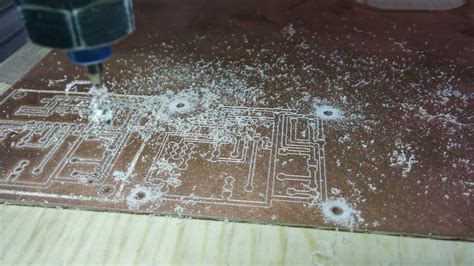
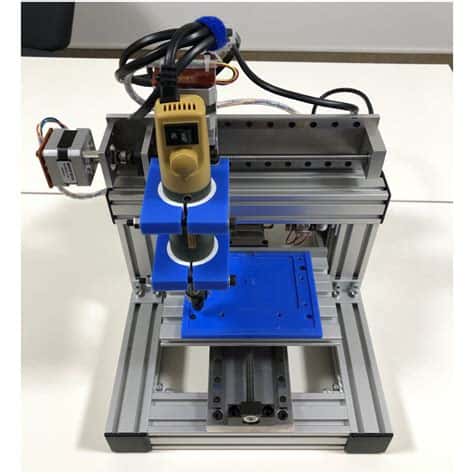
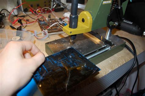
The Back Drilling Process
The back drilling process involves several steps to ensure precise and accurate removal of the unused portion of the PTHs. The process typically includes the following stages:
-
Design Preparation: The PCB design is analyzed to identify the locations of the PTHs that require back drilling. The design files are prepared, specifying the depth of the back drill for each hole location.
-
Drilling Depth Calculation: The depth of the back drill is calculated based on the thickness of the PCB, the location of the last inner layer, and the desired stub length. It is crucial to determine the correct drilling depth to ensure that the back drill removes the unused portion of the PTH without damaging the inner layers or the PTH itself.
-
Drill File Generation: Once the back drill depths are determined, a drill file is generated, containing the coordinates and depths of the holes to be back drilled. This drill file is used to program the drilling machine for accurate and precise drilling.
-
Drilling Machine Setup: The drilling machine is set up with the appropriate drill bits and parameters based on the drill file. The machine is calibrated to ensure accurate positioning and depth control.
-
Back Drilling Execution: The PCB is loaded into the drilling machine, and the back drilling process is executed according to the drill file. The machine precisely drills the holes to the specified depths, removing the unused portion of the PTHs from the backside of the PCB.
-
Cleaning and Inspection: After the back drilling process, the PCB is cleaned to remove any debris or burrs created during drilling. The board is then inspected to ensure that the back drilled holes meet the specified requirements, such as depth accuracy and hole quality.
Challenges and Considerations in Back Drilling
While back drilling offers significant benefits in terms of signal integrity and performance, it also presents certain challenges and considerations that must be addressed during the PCB manufacturing process:
-
Accuracy and Precision: Back drilling requires high accuracy and precision to ensure that the unused portion of the PTH is removed without damaging the inner layers or the PTH itself. Even a slight deviation in drilling depth can lead to inadequate stub removal or damage to the PCB. Advanced drilling machines with high-precision depth control and positioning systems are essential for successful back drilling.
-
Increased Manufacturing Time and Cost: Back drilling adds an additional step to the PCB manufacturing process, which can increase the overall production time and cost. The extra time required for design preparation, drill file generation, and the actual back drilling process can impact the manufacturing throughput. However, the benefits of improved signal integrity and performance often outweigh the added time and cost.
-
Material Selection: The choice of PCB substrate material can affect the back drilling process. Some materials, such as high-frequency laminates, may be more challenging to back drill due to their unique properties. The drilling parameters, such as feed rate and spindle speed, may need to be adjusted based on the material characteristics to ensure optimal results.
-
Hole Wall Quality: Back drilling can potentially affect the quality of the hole walls, especially if not executed properly. Rough hole walls or burrs created during the back drilling process can impact the signal integrity and reliability of the PCB. Proper drill bit selection, drilling parameters, and cleaning processes are crucial to maintain good hole wall quality.
-
Design Considerations: Designing a PCB for back drilling requires careful consideration of various factors, such as the placement of components, routing of traces, and the location of PTHs. The designer must ensure that the PTHs targeted for back drilling are accessible from the backside of the PCB and that there is sufficient clearance for the drilling process. Collaboration between the PCB design team and the manufacturing team is essential to optimize the design for back drilling.
Best Practices for Implementing Back Drilling
To ensure successful implementation of back drilling in PCB manufacturing, consider the following best practices:
-
Early Design Collaboration: Involve the PCB manufacturing team early in the design process to discuss the feasibility and requirements for back drilling. Early collaboration helps in identifying any design challenges and ensures that the PCB is optimized for back drilling.
-
Precise Drilling Depth Calculation: Accurately calculate the drilling depth for each PTH location based on the PCB stackup and the desired stub length. Use advanced PCB design tools and collaborate with the manufacturing team to determine the appropriate drilling depths.
-
Proper Drill Bit Selection: Choose the appropriate drill bits for back drilling based on the hole size, material type, and desired hole quality. Use high-quality, sharp drill bits to minimize hole wall roughness and ensure clean, burr-free holes.
-
Optimize Drilling Parameters: Adjust the drilling parameters, such as feed rate, spindle speed, and peck drilling settings, based on the material properties and hole characteristics. Optimize these parameters to achieve the desired hole quality and minimize any potential damage to the PCB.
-
Rigorous Inspection and Quality Control: Implement thorough inspection and quality control measures to verify the accuracy and quality of the back drilled holes. Use advanced inspection techniques, such as X-ray or cross-sectional analysis, to ensure that the drilling depths are within the specified tolerances and that the hole walls are of acceptable quality.
-
Continuous Process Improvement: Monitor and analyze the back drilling process regularly to identify any areas for improvement. Collect data on drilling performance, hole quality, and yields to drive continuous process optimization. Regularly review and update the back drilling procedures and parameters based on the feedback and analysis.
Conclusion
Back drilling is a critical PCB drilling technique that plays a vital role in enhancing signal integrity and reducing signal distortion in high-speed PCB designs. By removing the unused portion of PTHs, back drilling minimizes stub lengths, reduces impedance discontinuities, and mitigates crosstalk and EMI issues. While back drilling presents certain challenges, such as increased manufacturing time and cost, the benefits it offers in terms of improved PCB performance and reliability make it a valuable technique in the PCB manufacturing process.
To successfully implement back drilling, it is essential to collaborate closely with the PCB design and manufacturing teams, optimize the drilling process parameters, and adhere to best practices. By investing in advanced drilling equipment, skilled personnel, and rigorous quality control measures, PCB manufacturers can effectively incorporate back drilling into their processes and deliver high-quality, high-performance PCBs to meet the demands of modern electronic devices.
As technology continues to advance and the need for high-speed, high-performance electronic systems grows, the importance of back drilling in PCB manufacturing will only continue to increase. By understanding the principles, benefits, and challenges of back drilling, PCB designers and manufacturers can make informed decisions and implement this technique effectively to enhance the overall quality and reliability of their products.
FAQ
-
What is the purpose of back drilling in PCB manufacturing?
Back drilling is used to remove the unused portion of plated through-holes (PTHs) from the backside of a PCB. This helps in reducing stub lengths, minimizing signal reflections, and improving signal integrity in high-speed PCB designs. -
How does back drilling improve signal integrity?
Back drilling improves signal integrity by reducing the capacitance and inductance associated with the unused portion of PTHs. By removing the stubs, back drilling minimizes signal reflections, reduces impedance discontinuities, and mitigates crosstalk and EMI issues. -
Is back drilling suitable for all PCB designs?
Back drilling is particularly beneficial for high-speed PCB designs where signal integrity is critical. However, not all PCB designs require back drilling. The decision to implement back drilling depends on factors such as the signal speeds, PCB stackup, and performance requirements of the specific application. -
What are the challenges associated with back drilling?
Some of the challenges associated with back drilling include achieving accurate and precise drilling depths, maintaining good hole wall quality, and the increased manufacturing time and cost. Proper drill bit selection, optimized drilling parameters, and rigorous inspection and quality control measures are necessary to overcome these challenges. -
How can PCB designers optimize their designs for back drilling?
PCB designers can optimize their designs for back drilling by considering factors such as component placement, trace routing, and PTH locations. Early collaboration with the PCB manufacturing team, accurate drilling depth calculations, and adherence to design guidelines can help in creating designs that are well-suited for back drilling.
| Aspect | Importance |
|---|---|
| Signal Integrity | Back drilling reduces signal reflections, impedance discontinuities, crosstalk, and EMI |
| High-Speed Designs | Back drilling is critical for high-speed PCB designs to ensure reliable signal transmission |
| Stub Length Reduction | Back drilling minimizes stub lengths, reducing capacitance and inductance |
| Manufacturing Process | Back drilling adds an additional step to the PCB manufacturing process |
| Design Optimization | PCB designs must be optimized for back drilling through careful consideration of various factors |
No responses yet