Introduction
Signal integrity is a critical aspect of PCB design that ensures reliable and accurate transmission of signals between components. One key factor that can significantly impact signal integrity is the routing of tracks on adjacent layers of the PCB. Parallel track routing on adjacent layers can lead to crosstalk, electromagnetic interference (EMI), and other issues that can degrade signal quality and performance. In this article, we will explore the importance of avoiding adjacent layer parallel track routing and discuss best practices for optimizing signal integrity in PCB design.
Understanding Signal Integrity
What is Signal Integrity?
Signal integrity refers to the ability of an electrical signal to maintain its intended characteristics as it propagates through a system. In the context of PCB design, signal integrity is concerned with ensuring that the signals transmitted between components maintain their intended voltage levels, timing, and waveform shape. Maintaining good signal integrity is essential for reliable and accurate operation of electronic devices.
Factors Affecting Signal Integrity
Several factors can impact signal integrity in PCB design, including:
- Trace geometry: The width, thickness, and spacing of traces can affect impedance matching and signal propagation.
- Dielectric properties: The dielectric constant and loss tangent of the PCB substrate material can influence signal speed and attenuation.
- Crosstalk: Electromagnetic coupling between adjacent traces can cause crosstalk, leading to signal distortion and noise.
- Reflections: Impedance mismatches at trace junctions and terminations can cause signal reflections, resulting in ringing and overshoot.
- EMI: Electromagnetic interference from external sources or other components on the PCB can disrupt signal integrity.
Problems with Adjacent Layer Parallel Track Routing
Crosstalk
One of the primary issues with adjacent layer parallel track routing is crosstalk. Crosstalk occurs when a signal on one trace induces an unwanted voltage or current on an adjacent trace through capacitive or inductive coupling. This can lead to signal distortion, noise, and even false triggering of digital circuits. The severity of crosstalk depends on factors such as the spacing between traces, the length of parallel runs, and the frequency and rise/fall times of the signals.
Electromagnetic Interference (EMI)
Parallel track routing on adjacent layers can also contribute to EMI. When high-speed signals are routed in parallel, they can act as antennas, radiating electromagnetic energy that can interfere with nearby components or even cause compliance issues with electromagnetic compatibility (EMC) regulations. EMI can be particularly problematic in designs with sensitive analog circuits or wireless communication modules.
Impedance Mismatch
Routing tracks on adjacent layers can also create impedance mismatches, especially if the traces have different geometries or are not properly terminated. Impedance mismatches can cause signal reflections, leading to ringing, overshoot, and undershoot on the signal waveform. These issues can degrade signal quality and increase the likelihood of bit errors in digital communication.

Best Practices for Avoiding Adjacent Layer Parallel Track Routing
Route Signals on Different Layers
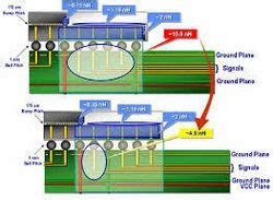
One of the most effective ways to avoid the problems associated with adjacent layer parallel track routing is to route signals on different layers of the PCB. By separating sensitive signals onto dedicated layers, you can minimize crosstalk and EMI. For example, you might route high-speed signals on an inner layer, sandwiched between ground planes, while routing lower-speed signals on outer layers.
Use Orthogonal Routing
When routing signals on adjacent layers is unavoidable, use orthogonal routing techniques to minimize the length of parallel runs. Orthogonal routing involves routing traces at right angles to each other, rather than in parallel. This helps to reduce the capacitive and inductive coupling between traces, thereby minimizing crosstalk.
Maintain Adequate Spacing
Ensure that there is sufficient spacing between traces on adjacent layers to reduce crosstalk and EMI. The spacing required depends on factors such as the signal frequency, rise/fall times, and the dielectric properties of the PCB substrate. As a general rule, aim for a spacing of at least 3 times the trace width for high-speed signals.
Use Guard Traces and Ground Planes
Incorporating guard traces and ground planes can help to shield sensitive signals from crosstalk and EMI. Guard traces are grounded traces that are placed adjacent to sensitive signal traces to provide shielding. Ground planes are continuous copper layers that are connected to ground and placed above and below signal layers to provide additional shielding and reduce EMI.
Implement Proper Termination
Ensuring proper termination of signal traces is crucial for minimizing reflections and maintaining signal integrity. Use appropriate termination techniques, such as series termination or parallel termination, based on the characteristics of the signals and the trace geometries. Proper termination helps to match the impedance of the traces to the source and load impedances, reducing reflections and improving signal quality.
Case Study: High-Speed Digital Design
To illustrate the importance of avoiding adjacent layer parallel track routing, let’s consider a case study of a high-speed digital design. Suppose you are designing a PCB for a high-performance digital system that includes a processor, memory, and various peripheral components. The design requires high-speed digital interfaces, such as DDR memory and PCIe, with signal speeds exceeding 1 GHz.
In this scenario, proper signal integrity is critical for ensuring reliable operation and preventing data corruption. By following best practices for avoiding adjacent layer parallel track routing, you can optimize the PCB layout for signal integrity:
- Route the high-speed signals, such as DDR and PCIe, on dedicated inner layers, sandwiched between ground planes. This helps to minimize crosstalk and EMI by providing shielding and reducing the influence of external noise sources.
- Use orthogonal routing techniques when routing signals on adjacent layers is necessary. For example, route the address and control signals of the DDR interface at right angles to the data signals to minimize parallel runs and reduce crosstalk.
- Maintain adequate spacing between traces on adjacent layers. For high-speed signals like DDR and PCIe, aim for a spacing of at least 3 times the trace width to minimize capacitive and inductive coupling.
- Incorporate guard traces and ground planes to provide additional shielding for sensitive signals. Place ground traces adjacent to critical signal traces and use continuous ground planes above and below the signal layers to reduce EMI.
- Implement proper termination for the high-speed interfaces. Use on-die termination (ODT) for DDR signals and appropriate termination resistors for PCIe signals to match the trace impedances and minimize reflections.
By following these guidelines and avoiding adjacent layer parallel track routing, you can ensure optimal signal integrity in your high-speed digital design, reducing the risk of signal distortion, crosstalk, and EMI-related issues.
Frequently Asked Questions (FAQ)
-
Q: What is the main reason to avoid adjacent layer parallel track routing?
A: The main reason to avoid adjacent layer parallel track routing is to minimize crosstalk and electromagnetic interference (EMI) between signals. Parallel routing on adjacent layers can lead to capacitive and inductive coupling, causing signal distortion and noise. -
Q: How can I minimize crosstalk when routing signals on adjacent layers?
A: To minimize crosstalk when routing signals on adjacent layers, you can use orthogonal routing techniques, maintaining adequate spacing between traces, and incorporating guard traces and ground planes for shielding. Orthogonal routing involves routing traces at right angles to each other to reduce the length of parallel runs. -
Q: What is the recommended spacing between traces on adjacent layers?
A: The recommended spacing between traces on adjacent layers depends on factors such as the signal frequency, rise/fall times, and the dielectric properties of the PCB substrate. As a general guideline, aim for a spacing of at least 3 times the trace width for high-speed signals to minimize crosstalk and EMI. -
Q: How can I reduce EMI in my PCB design?
A: To reduce EMI in your PCB design, you can follow several best practices, including routing sensitive signals on dedicated layers, using guard traces and ground planes for shielding, maintaining adequate spacing between traces, and implementing proper termination techniques. Additionally, consider using EMI filters, shielding enclosures, and following EMC guidelines. -
Q: What is the role of termination in maintaining signal integrity?
A: Proper termination is crucial for maintaining signal integrity by minimizing reflections and ensuring impedance matching between the source, trace, and load. Appropriate termination techniques, such as series termination or parallel termination, help to match the impedance of the traces to the source and load impedances, reducing signal reflections and improving signal quality.
Conclusion
Signal integrity is a critical consideration in PCB design, and avoiding adjacent layer parallel track routing is one of the key strategies for optimizing signal quality and minimizing issues like crosstalk and EMI. By following best practices such as routing signals on different layers, using orthogonal routing, maintaining adequate spacing, incorporating guard traces and ground planes, and implementing proper termination, designers can ensure reliable and accurate signal transmission in their PCB designs.
As electronic systems continue to push the boundaries of speed and complexity, maintaining signal integrity becomes increasingly challenging. By understanding the principles of signal integrity and applying appropriate design techniques, PCB designers can overcome these challenges and create robust, high-performance electronic devices that meet the demanding requirements of modern applications.
| Technique | Description | Benefits |
|---|---|---|
| Routing on Different Layers | Route sensitive signals on dedicated layers, separated from other signals | Minimizes crosstalk and EMI |
| Orthogonal Routing | Route traces at right angles to each other when routing on adjacent layers is necessary | Reduces the length of parallel runs and minimizes crosstalk |
| Adequate Spacing | Maintain sufficient spacing between traces on adjacent layers (e.g., 3 times the trace width for high-speed signals) | Reduces capacitive and inductive coupling, minimizing crosstalk and EMI |
| Guard Traces and Ground Planes | Use grounded traces adjacent to sensitive signals and continuous ground planes above and below signal layers | Provides shielding and reduces EMI |
| Proper Termination | Implement appropriate termination techniques (e.g., series or parallel termination) based on signal characteristics and trace geometries | Minimizes reflections, matches impedances, and improves signal quality |
By applying these techniques and avoiding adjacent layer parallel track routing, PCB designers can optimize signal integrity, ensuring reliable and robust performance in their electronic designs.
No responses yet