Antenna Design and RF Layout Guidelines
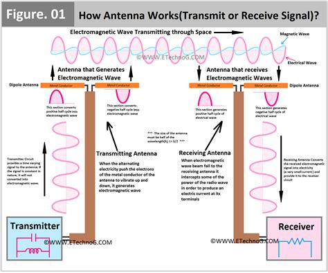
Introduction to Antenna Design and RF Layout Antenna design and RF layout are critical aspects of wireless communication systems. The antenna is responsible for transmitting[…]
Practical EMC Considerations in Designing PCB for RF and Microwave Communications Syste
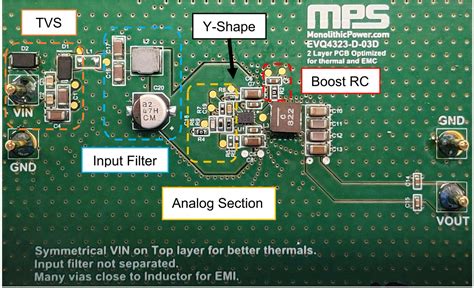
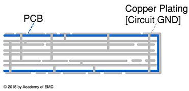
Introduction to EMC in PCB Design Electromagnetic Compatibility (EMC) is a critical aspect of designing printed circuit boards (PCBs) for RF and microwave communications systems.[…]
Ultimate Guide to EMC PCB Design and EMC Standards
Introduction to EMC PCB Design Electromagnetic Compatibility (EMC) is a critical aspect of printed circuit board (PCB) design that ensures electronic devices can function properly[…]
RAYMING Technologies: Advanced PCB Manufacturer & RF Supplier
About RAYMING Technologies RAYMING was founded in 1995 with the goal of becoming a premier PCB and RF supplier. Over the past 25+ years, the[…]

PCB Tips & Tricks
Understanding the Basics of PCB Design Before diving into advanced PCBHacks, it’s essential to have a solid foundation in PCB design basics. Let’s review some[…]
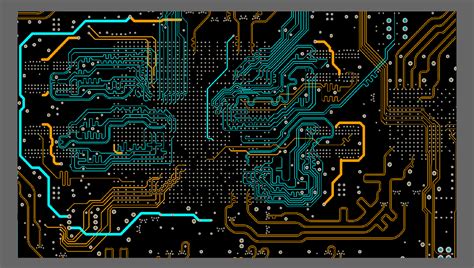
Analog, RF and EMC Considerations in Printed Circuit Board (PCB) Design
Introduction to PCB Design Printed Circuit Board (PCB) design is a crucial aspect of electronic product development, as it determines the functionality, reliability, and performance[…]
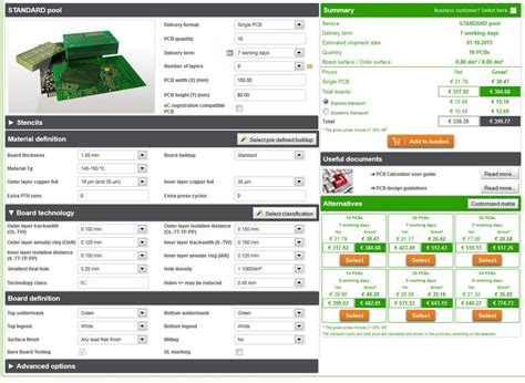
Guide to the Rayming PCB Calculator – calculate prices, get quotations, analyse your data
Introduction to the Rayming PCB Calculator The Rayming PCB Calculator is an essential tool for anyone looking to get accurate pricing and quotations for their[…]
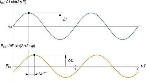
Defining Defined Impedance
What is Defined Impedance? Defined impedance, also known as controlled impedance or specified impedance, refers to the precise control and matching of impedance values in[…]
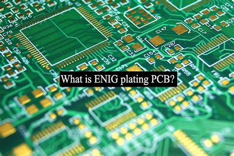
What is Che Ni/Au or ENIG?
Introduction to ENIG (Electroless Nickel Immersion Gold) ENIG, which stands for Electroless Nickel Immersion Gold, is a popular surface finish used in the manufacturing of[…]
Plating Simulation – our New Tool for PCB Designers
Introduction to PCB Plating Simulation Printed Circuit Board (PCB) design is a complex process that involves multiple steps, from schematic design to component placement, routing,[…]