What is PCB wire strain relief?
PCB wire strain relief is a technique used to protect the electrical connections between wires and printed circuit boards (PCBs) from mechanical stress and strain. It involves using various methods and components to secure the wires and prevent them from being pulled, twisted, or bent in a way that could damage the connections or cause the wires to break.
Types of PCB wire strain relief
There are several types of PCB wire strain relief methods and components, including:
- Strain relief clamps
- Cable ties
- Adhesive-backed mounts
- Grommets
- Shrink tubing
- Potting compounds
Each of these methods has its own advantages and disadvantages, and the choice of which one to use depends on factors such as the size and type of wires, the environmental conditions, and the level of strain relief required.
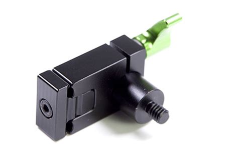
Strain relief clamps
Strain relief clamps are mechanical devices that are designed to grip and secure wires or cables to a PCB. They typically consist of two parts: a base that is mounted to the PCB and a cover that clamps down on the wires. Strain relief clamps come in various sizes and shapes to accommodate different wire gauges and cable diameters.
| Advantage | Disadvantage |
|---|---|
| Provides strong and secure strain relief | Requires additional space on the PCB |
| Easy to install and remove | May not be suitable for high-density layouts |
| Suitable for a wide range of wire gauges | Can be relatively expensive |
Cable ties
Cable ties, also known as zip ties, are a simple and inexpensive way to provide strain relief for PCB wires. They are thin, flexible straps with a locking mechanism that allows them to be wrapped around a bundle of wires and tightened to hold them securely in place. Cable ties can be attached to the PCB using adhesive-backed mounts or through holes.
| Advantage | Disadvantage |
|---|---|
| Inexpensive and readily available | May not provide as much strain relief as other methods |
| Easy to install and remove | Can be difficult to adjust the tension |
| Suitable for small to medium-sized wires | May not be suitable for high-temperature applications |
Adhesive-backed mounts
Adhesive-backed mounts are small plastic or metal components that have a pressure-sensitive adhesive on one side and a means of attaching wires or cable ties on the other. They can be stuck directly to the surface of a PCB to provide a secure anchor point for strain relief. Adhesive-backed mounts come in various shapes and sizes, such as loops, hooks, and cable tie mounts.
| Advantage | Disadvantage |
|---|---|
| Easy to install without requiring holes in the PCB | May not provide as strong a bond as mechanical fasteners |
| Can be placed almost anywhere on the PCB surface | Not suitable for high-temperature or high-humidity environments |
| Suitable for small to medium-sized wires | May not be reusable if the adhesive loses its strength |
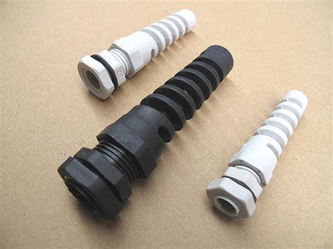
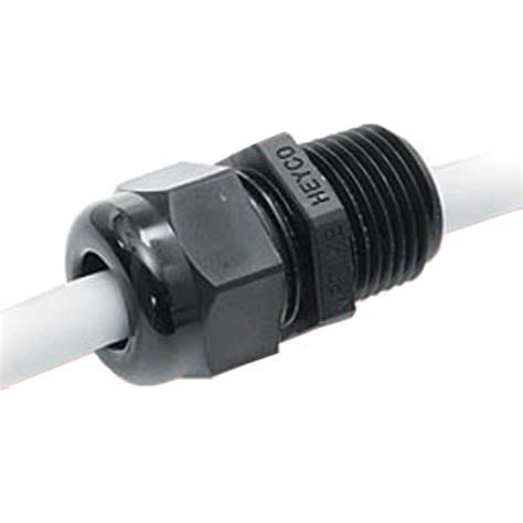
Grommets
Grommets are rubber or plastic rings that are inserted into holes in the PCB to provide a protective barrier and strain relief for wires passing through the holes. They have a slit or opening on one side that allows wires to be inserted or removed easily. Grommets come in various sizes to fit different hole diameters and wire gauges.
| Advantage | Disadvantage |
|---|---|
| Provides a neat and tidy appearance | Requires holes to be drilled in the PCB |
| Protects wires from sharp edges of the holes | May not provide as much strain relief as other methods |
| Suitable for a wide range of wire gauges | Can be difficult to insert and remove wires |
Shrink tubing
Shrink tubing is a flexible plastic tube that is designed to shrink and conform tightly to the shape of wires or components when heated. It can be used to provide strain relief for PCB wires by encapsulating the soldered connections and a portion of the wires. Shrink tubing is available in various sizes, colors, and materials to suit different applications.
| Advantage | Disadvantage |
|---|---|
| Provides a tight and secure fit around wires | Requires heat to shrink, which may not be suitable for some components |
| Insulates and protects the connections from moisture and debris | May not provide as much mechanical strength as other methods |
| Can be easily removed by cutting | May not be reusable once shrunk |
Potting compounds
Potting compounds are liquid or semi-liquid materials that are poured or injected around components and wires on a PCB to provide a protective encapsulation and strain relief. They are typically made from epoxy, silicone, or urethane and can be formulated with various properties such as high thermal conductivity, electrical insulation, and resistance to moisture and chemicals.
| Advantage | Disadvantage |
|---|---|
| Provides a complete and uniform encapsulation | Requires a mold or dam to contain the liquid compound |
| Can fill in gaps and voids around components | May be difficult to remove or rework once cured |
| Can provide excellent environmental protection | May have a long curing time and require special handling |
Factors to consider when selecting PCB wire strain relief
When selecting a PCB wire strain relief method, there are several factors to consider, including:
- Wire gauge and type
- Environmental conditions
- Mechanical stress and strain
- PCB Layout and space constraints
- Cost and availability
Wire gauge and type
The size and type of wires used in a PCB Assembly will influence the choice of strain relief method. Thicker wires and cables may require stronger and larger strain relief components, while thinner wires may be adequately secured with smaller and simpler methods. The insulation material of the wires should also be considered, as some materials may not be compatible with certain adhesives or potting compounds.
Environmental conditions
The environmental conditions in which the PCB will be used should also be taken into account when selecting a strain relief method. Factors such as temperature, humidity, vibration, and chemical exposure can affect the performance and durability of the strain relief components. For example, high temperatures may cause adhesives to lose their strength, while high humidity may cause corrosion of metal parts.
Mechanical stress and strain
The level of mechanical stress and strain that the PCB wires will be subjected to should also be considered. Applications that involve frequent plugging and unplugging of cables, or exposure to high levels of vibration or shock, may require more robust strain relief methods such as clamps or potting compounds. On the other hand, applications with minimal stress and strain may be adequately served by simpler methods such as cable ties or adhesive mounts.
PCB layout and space constraints
The layout and space constraints of the PCB should also be taken into account when selecting a strain relief method. Some methods, such as strain relief clamps, may require additional space on the PCB and may not be suitable for high-density layouts. Other methods, such as adhesive mounts or shrink tubing, may be more space-efficient but may not provide as much mechanical strength.
Cost and availability
Finally, the cost and availability of the strain relief components should be considered. Some methods, such as potting compounds or custom-designed clamps, may be more expensive and may have longer lead times than off-the-shelf components such as cable ties or grommets. The overall cost of the strain relief solution should be balanced against the required level of performance and reliability.
Best practices for PCB wire strain relief
To ensure effective and reliable PCB wire strain relief, there are several best practices that should be followed, including:
- Use the appropriate strain relief method for the application
- Provide adequate slack in the wires
- Secure the wires close to the PCB
- Use high-quality components and materials
- Test and validate the strain relief design
Use the appropriate strain relief method for the application
As discussed earlier, there are several strain relief methods available, each with its own advantages and disadvantages. It is important to select the method that is most appropriate for the specific application, taking into account factors such as wire size, environmental conditions, and mechanical stress.
Provide adequate slack in the wires
To prevent the wires from being subjected to excessive stress and strain, it is important to provide adequate slack between the PCB and the strain relief point. This allows the wires to flex and move without putting undue tension on the connections. The amount of slack required will depend on the application and the expected level of movement or vibration.
Secure the wires close to the PCB
To minimize the stress on the solder joints and PCB traces, it is important to secure the wires as close to the PCB as possible. This reduces the lever arm effect and distributes the stress more evenly across the connection. Strain relief components should be placed as close to the PCB as practical, without interfering with other components or obstructing access for assembly or maintenance.
Use high-quality components and materials
To ensure reliable and long-lasting strain relief, it is important to use high-quality components and materials that are designed for the specific application. This includes using wire and cable with appropriate insulation and conductor materials, as well as strain relief components that are made from durable and compatible materials. Cheap or low-quality components may save money in the short term but can lead to premature failure and costly repairs in the long run.
Test and validate the strain relief design
Before putting a PCB assembly into production, it is important to test and validate the strain relief design to ensure that it meets the required performance and reliability criteria. This may involve subjecting the assembly to simulated environmental and mechanical stresses, such as temperature cycling, vibration, and pull tests. Any weaknesses or failures identified during testing should be addressed and corrected before the design is finalized.

Frequently Asked Questions (FAQ)
- What is the most common method of PCB wire strain relief?
-
The most common method of PCB wire strain relief is the use of strain relief clamps or cable ties. These methods are simple, inexpensive, and effective for most applications.
-
Can PCB wire strain relief be added after the assembly is complete?
-
In some cases, strain relief can be added after the assembly is complete, such as by using adhesive-backed mounts or shrink tubing. However, it is generally better to incorporate strain relief into the initial design and assembly process to ensure proper placement and security.
-
How much slack should be provided in the wires for strain relief?
-
The amount of slack required for strain relief depends on the application and the expected level of movement or vibration. As a general rule, there should be enough slack to allow the wires to flex and move without putting excessive tension on the connections, but not so much that the wires can become tangled or snagged.
-
Can potting compounds be used for strain relief on all types of PCBs?
-
Potting compounds can be used for strain relief on most types of PCBs, but they may not be suitable for all applications. Potting compounds can add significant weight and volume to the assembly, and may not be compatible with certain components or materials. It is important to carefully consider the specific requirements of the application before using potting compounds for strain relief.
-
How can I test the effectiveness of my PCB wire strain relief design?
- To test the effectiveness of a PCB wire strain relief design, you can subject the assembly to simulated environmental and mechanical stresses, such as temperature cycling, vibration, and pull tests. These tests can help to identify any weaknesses or failures in the strain relief design and allow for corrective action to be taken before the assembly is put into production. It is also important to regularly inspect and maintain the strain relief components during the lifetime of the product to ensure continued performance and reliability.
Conclusion
PCB wire strain relief is a critical aspect of designing and manufacturing reliable and durable electronic assemblies. By understanding the various methods and components available for strain relief, and by following best practices for design and implementation, engineers and technicians can ensure that their PCB assemblies can withstand the rigors of real-world use and provide long-lasting performance. Whether using simple cable ties or advanced potting compounds, the key is to select the most appropriate strain relief solution for the specific application and to validate the design through thorough testing and inspection.
No responses yet