Introduction to PCB Manufacturing
Printed Circuit Boards (PCBs) are the backbone of modern electronics, providing a platform for interconnecting electronic components in a compact and efficient manner. The PCB manufacturing process involves a series of complex steps that transform a design concept into a functional, reliable board. One increasingly popular type of PCB is the Aluminum PCB, which offers unique advantages such as excellent thermal dissipation and mechanical stability.
In this article, we will delve into the aluminum PCB manufacturing process within a PCB factory, exploring each step in detail and discussing the benefits and challenges associated with this specialized manufacturing technique.
Understanding Aluminum PCBs
What are Aluminum PCBs?
Aluminum PCBs are a type of printed circuit board that utilizes an aluminum substrate instead of the traditional FR-4 material. The aluminum substrate serves as both a structural support and a heat dissipation medium, making these PCBs ideal for applications that generate significant amounts of heat, such as high-power electronics, LED lighting, and automotive systems.
Advantages of Aluminum PCBs
Aluminum PCBs offer several key advantages over traditional FR-4 PCBs:
-
Excellent thermal conductivity: Aluminum has a high thermal conductivity, allowing it to efficiently transfer heat away from electronic components, thus improving the overall thermal management of the system.
-
Enhanced mechanical stability: The aluminum substrate provides a rigid and durable base for the PCB, reducing the risk of warping or damage during handling and operation.
-
Lightweight construction: Despite their strength, aluminum PCBs are relatively lightweight compared to other metal-core PCBs, making them suitable for weight-sensitive applications.
-
Cost-effective: Aluminum is an abundant and affordable material, making aluminum PCBs a cost-effective solution for many applications.

Aluminum PCB Manufacturing Process
The aluminum PCB manufacturing process consists of several critical steps, each of which contributes to the final quality and functionality of the board. Let’s explore these steps in detail.
Step 1: Design and Preparation
The first step in the aluminum PCB manufacturing process is the design and preparation phase. This involves creating a detailed schematic and layout of the PCB using specialized software tools such as Altium Designer, Eagle, or KiCad. The design must take into account the specific requirements of the aluminum substrate, including thermal management, mechanical constraints, and dielectric properties.
Once the design is finalized, the data is converted into a format suitable for manufacturing, typically Gerber files or ODB++. These files contain all the necessary information for each layer of the PCB, including the copper traces, solder mask, silkscreen, and drill holes.
Step 2: Aluminum Substrate Preparation
The next step is to prepare the aluminum substrate. This involves cutting the aluminum sheet to the desired size and shape using precise CNC machines. The surface of the aluminum is then cleaned and treated to improve adhesion with the upcoming layers.
A common surface treatment method is chemical etching, which creates a roughened surface that enhances the bonding strength between the aluminum and the dielectric layer. Another option is anodizing, which forms a thin, protective oxide layer on the aluminum surface, improving corrosion resistance and electrical insulation.
Step 3: Applying the Dielectric Layer
The dielectric layer is a critical component of an aluminum PCB, as it provides electrical insulation between the aluminum substrate and the copper traces. The most common dielectric materials used in aluminum PCBs are:
-
Polyimide: A high-temperature, flexible polymer with excellent electrical and mechanical properties.
-
Epoxy: A thermosetting polymer known for its strong adhesion, chemical resistance, and thermal stability.
-
Ceramic: A high-performance, inorganic material with exceptional thermal conductivity and electrical insulation properties.
The dielectric layer is typically applied using a lamination process, where the material is pressed onto the aluminum substrate under high temperature and pressure. The thickness of the dielectric layer must be carefully controlled to ensure proper electrical insulation and thermal conductivity.
Step 4: Drilling and Plating
Once the dielectric layer is in place, the next step is to drill holes in the PCB for through-hole components and vias. This is done using high-speed, computer-controlled drilling machines that can create holes with diameters as small as 0.1mm.
After drilling, the holes are plated with copper to create electrical connections between the layers of the PCB. This is typically done using an electroplating process, where the board is immersed in a copper sulfate solution and an electric current is applied, causing copper to deposit onto the exposed surfaces of the holes.
Step 5: Copper Patterning
The copper patterning step is where the actual circuitry of the PCB is created. This involves applying a thin layer of copper onto the dielectric layer, typically using an electroless copper deposition process or a direct bonding copper (DBC) technique.
Once the copper layer is in place, it is patterned using a photolithography process. This involves applying a light-sensitive photoresist material onto the copper layer, exposing it to UV light through a photomask that contains the desired circuit pattern, and then developing the photoresist to remove the exposed areas.
The exposed copper is then etched away using a chemical etching solution, leaving behind the desired copper traces and pads. This process is repeated for each layer of the PCB, with careful alignment between the layers to ensure proper connectivity.
Step 6: Solder Mask Application
The solder mask is a protective layer that covers the copper traces and pads on the PCB, leaving only the areas intended for soldering exposed. This layer serves several purposes, including:
- Protecting the copper from oxidation and corrosion
- Preventing accidental short circuits during soldering
- Providing a visual guide for component placement and soldering
The solder mask is typically applied using a screen printing process, where the liquid solder mask material is forced through a fine mesh screen onto the PCB surface. The solder mask is then cured using UV light or heat to form a durable, protective layer.
Step 7: Surface Finish Application
The surface finish is the final protective layer applied to the exposed copper areas of the PCB, such as pads and through-holes. The purpose of the surface finish is to:
- Protect the copper from oxidation and corrosion
- Enhance the solderability of the copper surfaces
- Improve the electrical and mechanical reliability of the connections
Common surface finish options for aluminum PCBs include:
-
Hot Air Solder Leveling (HASL): A process where the PCB is dipped in molten solder and then leveled using hot air knives, creating a flat, solderable surface.
-
Electroless Nickel Immersion Gold (ENIG): A two-step process that involves depositing a layer of nickel onto the copper, followed by a thin layer of gold. ENIG provides excellent solderability, corrosion resistance, and durability.
-
Immersion Silver: A simple and cost-effective process where the copper surfaces are coated with a thin layer of silver, providing good solderability and moderate corrosion resistance.
Step 8: Silk Screen Printing
Silk screen printing is the process of applying the text, logos, and other markings onto the PCB surface. This is typically done using a screen printing process similar to the solder mask application, where ink is forced through a fine mesh screen onto the PCB surface.
The silk screen layer serves several purposes, including:
- Providing a visual reference for component placement and orientation
- Displaying important information such as part numbers, version codes, and company logos
- Enhancing the overall aesthetics of the PCB
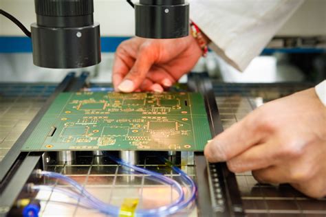
Step 9: Final Inspection and Testing
Once all the layers of the aluminum PCB have been completed, the board undergoes a thorough final inspection and testing process to ensure its quality and functionality. This typically involves:
- Visual inspection: Checking for any visible defects, such as scratches, dents, or discoloration
- Automated Optical Inspection (AOI): Using high-resolution cameras and computer vision algorithms to detect any missing or misaligned components, solder bridging, or other manufacturing defects
- Electrical testing: Verifying the electrical continuity and insulation resistance of the PCB using specialized test equipment, such as Flying Probe testers or bed-of-nails fixtures
- Thermal testing: Ensuring that the aluminum PCB can effectively dissipate heat under various operating conditions, using thermal imaging cameras or thermocouples
Boards that pass the final inspection and testing are then packaged and shipped to the customer, while any defective boards are either reworked or scrapped, depending on the nature and severity of the defects.

Benefits of Aluminum PCBs in Various Applications
Aluminum PCBs offer unique advantages that make them well-suited for a wide range of applications, particularly those that involve high power densities, extreme operating temperatures, or harsh environmental conditions. Some of the key benefits of using aluminum PCBs in various applications include:
Improved Thermal Management
One of the primary advantages of aluminum PCBs is their excellent thermal conductivity, which allows them to efficiently dissipate heat away from electronic components. This is particularly important in applications such as:
-
Power electronics: High-power devices like IGBTs, MOSFETs, and rectifiers generate significant amounts of heat during operation, which must be effectively removed to prevent overheating and premature failure. Aluminum PCBs provide a direct thermal path from the components to the heatsink or cooling system, minimizing thermal resistance and improving overall system reliability.
-
LED lighting: High-brightness LEDs generate a substantial amount of heat, which can degrade their performance and lifespan if not properly managed. Aluminum PCBs help to spread the heat evenly across the board and transfer it to the heatsink or ambient environment, maintaining optimal LED temperature and ensuring consistent light output.
-
Automotive electronics: Modern vehicles rely on a wide range of electronic systems, many of which are subjected to high temperatures and vibrations. Aluminum PCBs offer a rugged and thermally stable platform for automotive applications such as engine control modules, power inverters, and battery management systems, ensuring reliable operation in demanding environments.
Enhanced Mechanical Stability
Aluminum PCBs provide a rigid and durable substrate that can withstand the mechanical stresses and vibrations encountered in various applications. This is especially important in:
-
Aerospace and defense systems: Electronic systems used in aircraft, satellites, and military equipment must be able to withstand extreme temperature fluctuations, vibrations, and shock loads. Aluminum PCBs offer a robust and lightweight solution that can meet the stringent reliability requirements of these applications.
-
Industrial automation: Factory automation systems, such as robotics and machine vision, require PCBs that can operate reliably in harsh industrial environments, where they may be exposed to dust, moisture, and vibrations. Aluminum PCBs provide a stable and durable platform that can withstand these conditions, minimizing downtime and maintenance costs.
-
Outdoor applications: Electronic systems used in outdoor environments, such as solar inverters, wind turbine controls, and telecommunications equipment, must be able to withstand extreme temperature variations, humidity, and UV exposure. Aluminum PCBs offer a corrosion-resistant and thermally stable solution that can ensure reliable operation in these challenging conditions.
Cost-Effective Manufacturing
Aluminum PCBs can be a cost-effective solution for many applications, particularly those that require high thermal performance or mechanical stability. Some of the key cost advantages of aluminum PCBs include:
-
Reduced heatsink requirements: The excellent thermal conductivity of aluminum PCBs can often eliminate the need for separate heatsinks or cooling systems, reducing the overall system cost and complexity.
-
Simplified assembly: Aluminum PCBs can be designed with integrated mounting features, such as threaded inserts or mounting holes, which can simplify the assembly process and reduce the need for additional hardware.
-
Longer system lifespan: The enhanced thermal and mechanical properties of aluminum PCBs can help to extend the lifespan of electronic components and systems, reducing maintenance and replacement costs over time.

Challenges and Considerations in Aluminum PCB Manufacturing
While aluminum PCBs offer many benefits, there are also some unique challenges and considerations that must be addressed during the manufacturing process. Some of the key challenges include:
Thermal Expansion Mismatch
One of the main challenges in aluminum PCB manufacturing is the mismatch in thermal expansion coefficients between the aluminum substrate and the copper traces. Aluminum has a higher coefficient of thermal expansion (CTE) than copper, which can lead to stress and deformation of the copper traces during temperature cycling.
To mitigate this issue, manufacturers must carefully select the dielectric material and thickness to provide a buffer between the aluminum and copper layers. In some cases, a special low-CTE copper alloy may be used to better match the thermal expansion of the aluminum substrate.
Dielectric Material Selection
The choice of dielectric material is critical in aluminum PCB manufacturing, as it must provide sufficient electrical insulation, thermal conductivity, and mechanical adhesion to the aluminum substrate. Common dielectric materials used in aluminum PCBs include:
-
Polyimide: A high-performance polymer with excellent thermal stability and electrical insulation properties, but relatively low thermal conductivity.
-
Epoxy: A widely used dielectric material that offers good adhesion and thermal stability, but may have limited thermal conductivity and high-temperature performance.
-
Ceramic: An inorganic dielectric material with excellent thermal conductivity and electrical insulation properties, but can be brittle and more expensive than polymer options.
Manufacturers must carefully consider the specific requirements of the application, such as operating temperature range, power density, and cost, when selecting the appropriate dielectric material for an aluminum PCB.
Surface Treatment and Bonding
To ensure reliable adhesion between the aluminum substrate and the dielectric layer, the surface of the aluminum must be properly treated and cleaned prior to bonding. Common surface treatment methods include:
-
Chemical etching: A process that uses acidic or alkaline solutions to create a micro-roughened surface on the aluminum, improving adhesion with the dielectric layer.
-
Anodizing: An electrochemical process that forms a thin, porous oxide layer on the aluminum surface, providing improved corrosion resistance and adhesion.
-
Plasma treatment: A dry process that uses ionized gas to clean and activate the aluminum surface, enhancing adhesion without the use of wet chemicals.
The choice of surface treatment method will depend on the specific dielectric material being used, as well as the performance and reliability requirements of the application.
Thermal Management Design
While aluminum PCBs offer excellent thermal conductivity, proper thermal management design is still critical to ensure optimal heat dissipation and prevent hot spots on the board. Some key considerations in aluminum PCB thermal management design include:
-
Component placement: High-power components should be placed strategically on the board to minimize thermal interaction and ensure even heat distribution.
-
Copper thickness: Thicker copper traces can help to improve thermal conductivity and spread heat more evenly across the board.
-
Thermal vias: The use of thermal vias, which are small holes filled with thermally conductive material, can help to transfer heat from the components to the aluminum substrate more efficiently.
-
Heatsink integration: In some cases, the aluminum PCB can be designed with an integrated heatsink or thermal interface material to further enhance heat dissipation.
Proper thermal management design requires close collaboration between the PCB designer, manufacturer, and end-user to ensure that the aluminum PCB can meet the specific thermal requirements of the application.
FAQ
- What are the main advantages of using aluminum PCBs compared to traditional FR-4 PCBs?
Aluminum PCBs offer several key advantages over FR-4 PCBs, including:
– Excellent thermal conductivity for improved heat dissipation
– Enhanced mechanical stability and durability
– Lightweight construction for weight-sensitive applications
– Cost-effective solution for high-performance applications
- What are the most common dielectric materials used in aluminum PCBs?
The most common dielectric materials used in aluminum PCBs are:
– Polyimide: A high-temperature, flexible polymer with excellent electrical and mechanical properties
– Epoxy: A thermosetting polymer known for its strong adhesion, chemical resistance, and thermal stability
– Ceramic: A high-performance, inorganic material with exceptional thermal conductivity and electrical insulation properties
- How does the thermal expansion mismatch between aluminum and copper affect the manufacturing process?
The mismatch in thermal expansion coefficients between aluminum and copper can lead to stress and deformation of the copper traces during temperature cycling. To mitigate this issue, manufacturers must carefully select the dielectric material and thickness to provide a buffer between the aluminum and copper layers, and in some cases, use special low-CTE copper alloys.
- What surface treatment methods are used to improve adhesion between the aluminum substrate and the dielectric layer?
Common surface treatment methods for aluminum PCBs include:
– Chemical etching: Using acidic or alkaline solutions to create a micro-roughened surface on the aluminum
– Anodizing: An electrochemical process that forms a thin, porous oxide layer on the aluminum surface
– Plasma treatment: A dry process that uses ionized gas to clean and activate the aluminum surface
- What are some key considerations in aluminum PCB thermal management design?
Some key considerations in aluminum PCB thermal management design include:
– Strategic component placement to minimize thermal interaction and ensure even heat distribution
– Using thicker copper traces to improve thermal conductivity and spread heat more evenly across the board
– Incorporating thermal vias to transfer heat from the components to the aluminum substrate more efficiently
– Designing the aluminum PCB with an integrated heatsink or thermal interface material to further enhance heat dissipation
Conclusion
Aluminum PCBs offer a unique combination of thermal, mechanical, and electrical properties that make them an attractive solution for a wide range of high-performance applications. By leveraging the excellent thermal conductivity and mechanical stability of aluminum, along with advanced manufacturing techniques and materials, PCB manufacturers can create boards that can withstand the
No responses yet