Introduction to PCB Stencils
PCB stencils are an essential tool in the electronics manufacturing process. They are used to apply solder paste onto printed circuit boards (PCBs) before component placement and soldering. The use of stencils ensures precise and consistent solder paste application, which is crucial for achieving reliable and high-quality solder joints.
What are PCB Stencils?
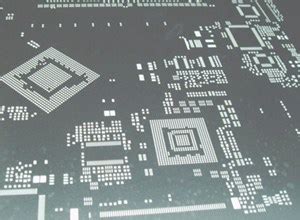
PCB stencils are thin metal sheets, typically made of stainless steel or nickel, with laser-cut openings that correspond to the solder pad locations on a PCB. The openings allow solder paste to be deposited onto the pads when the stencil is placed over the PCB and solder paste is applied using a squeegee.
Benefits of Using PCB Stencils
Using PCB stencils offers several benefits in the PCB Assembly process:
- Precise solder paste application: Stencils ensure that the correct amount of solder paste is deposited on each pad, reducing the risk of insufficient or excessive solder.
- Consistent results: Stencils provide consistent solder paste application across multiple PCBs, ensuring uniformity in the manufacturing process.
- Increased efficiency: Using stencils is much faster than applying solder paste manually, making the assembly process more efficient.
- Improved quality: Precise solder paste application leads to better solder joint quality, reducing the risk of defects and improving the overall reliability of the assembLED PCBs.
Types of PCB Stencils
There are several types of PCB stencils available, each with its own characteristics and applications.
Stainless Steel Stencils
Stainless steel stencils are the most common type of PCB stencils. They are durable, long-lasting, and suitable for high-volume production. Stainless steel stencils are typically laser-cut to ensure precise openings and smooth edges.
Nickel Stencils
Nickel stencils are an alternative to stainless steel stencils. They offer similar durability and precision but have a slightly different surface finish. Nickel stencils are often used in applications where a specific surface finish is required, such as in the automotive or aerospace industries.
Polyimide Stencils
Polyimide stencils, also known as polymer stencils, are made of a flexible, non-metallic material. They are suitable for applications where the stencil needs to conform to irregular surfaces or when a non-conductive stencil is required. Polyimide stencils are less durable than metal stencils and are typically used for low-volume or prototype production.
Step Stencils
Step stencils, also called multi-level stencils, have different thicknesses in different areas of the stencil. This allows for the application of different amounts of solder paste on different components, such as fine-pitch and larger components on the same PCB. Step stencils are useful for PCBs with a mix of component sizes and types.

Stencil Design Considerations
Proper stencil design is crucial for achieving optimal results in the solder paste application process. Several factors should be considered when designing a PCB stencil.
Aperture Size and Shape
The size and shape of the stencil apertures (openings) should be carefully designed to ensure the correct amount of solder paste is deposited on each pad. The aperture size is typically slightly larger than the pad size to account for the solder paste shrinkage during the reflow process.
Common aperture shapes include:
– Square: Used for most standard SMD pads
– Circular: Used for round pads, such as those for BGA components
– Rectangular: Used for elongated pads, such as those for connectors or large components
Stencil Thickness
The thickness of the stencil determines the amount of solder paste deposited on the pads. Thicker stencils deposit more solder paste, while thinner stencils deposit less. The optimal stencil thickness depends on the component types, pad sizes, and the desired solder joint profile.
Typical stencil thicknesses range from 0.1 mm to 0.2 mm (4 to 8 mils), with 0.15 mm (6 mils) being a common choice for most applications.
Aperture Walls
The walls of the stencil apertures should be designed to facilitate the release of the solder paste onto the pads. Aperture walls can be straight or tapered, with tapered walls providing better paste release and reducing the risk of clogging.
Fiducial Marks
Fiducial marks are reference points on the stencil that align with corresponding marks on the PCB. They ensure proper alignment between the stencil and the PCB during the solder paste application process. Fiducial marks should be included in the stencil design and placed in locations that do not interfere with the component placement.

Stencil Manufacturing Process
The manufacturing process for PCB stencils involves several steps to ensure high quality and precision.
Laser Cutting
Most PCB stencils are manufactured using laser cutting technology. A high-powered laser is used to cut the stencil apertures according to the designed pattern. Laser cutting ensures precise and clean-cut edges, reducing the risk of solder paste bleeding or clogging.
Chemical Etching
Chemical etching is another method for manufacturing PCB stencils, particularly for larger apertures or thicker stencils. In this process, the stencil material is coated with a photoresist, exposed to UV light through a photomask, and then chemically etched to create the apertures. Chemical etching is less common than laser cutting due to its lower precision and longer processing time.
Electropolishing
After the stencil is cut or etched, it undergoes an electropolishing process to remove any burrs or rough edges. Electropolishing also improves the surface finish of the stencil, making it smoother and more resistant to solder paste adhesion.
Inspection and Quality Control
Before the stencil is shipped to the customer, it undergoes a thorough inspection and quality control process. This includes checking the aperture sizes, positions, and wall quality, as well as verifying the overall dimensions of the stencil. Automated optical inspection (AOI) systems are often used to ensure the stencil meets the required specifications.

Stencil Maintenance and Cleaning
Proper maintenance and cleaning of PCB stencils are essential for ensuring consistent solder paste application and extending the stencil’s lifespan.
Cleaning Methods
Stencils should be cleaned regularly to remove any residual solder paste or debris that can clog the apertures or affect the paste release. Common cleaning methods include:
- Manual cleaning: Using solvents and wiping the stencil with a lint-free cloth
- Ultrasonic cleaning: Immersing the stencil in an ultrasonic bath with a cleaning solution
- Automated cleaning: Using specialized stencil cleaning machines that combine solvent application, brushing, and drying
Storage and Handling
When not in use, stencils should be stored in a clean, dry environment to prevent damage or contamination. Stencils should be handled carefully to avoid bending, warping, or scratching the surface. Proper storage and handling can significantly extend the lifespan of a stencil.
Advanced PCB Stencil Services
As the electronics industry evolves, PCB stencil manufacturers are offering advanced services to meet the growing demands of customers.
Custom Stencil Design
Many stencil manufacturers offer custom stencil design services to help customers optimize their solder paste application process. This includes assistance with aperture size and shape selection, stencil thickness recommendations, and design reviews to ensure manufacturability and performance.
Rapid Prototyping
For customers who need stencils quickly for prototyping or low-volume production, some manufacturers offer rapid prototyping services. These services provide fast turnaround times, often within 24 to 48 hours, allowing customers to iterate on their designs and bring products to market faster.
Stencil Coating
Stencil coating services apply a thin layer of material, such as nano-coating or PTFE (polytetrafluoroethylene), to the stencil surface. These coatings improve the solder paste release characteristics, reduce the need for frequent cleaning, and extend the stencil’s lifespan. Coated stencils are particularly useful for high-volume production or when using difficult-to-print solder pastes.
Stencil Traceability
Some stencil manufacturers offer traceability services, which involve marking each stencil with a unique identification code. This code can be used to track the stencil throughout its lifecycle, from manufacturing to usage and maintenance. Traceability is important for quality control and process optimization, allowing customers to identify and address any issues related to specific stencils.
Choosing a PCB Stencil Manufacturer
When selecting a PCB stencil manufacturer, several factors should be considered to ensure high-quality stencils and reliable service.
Manufacturing Capabilities
Choose a manufacturer with state-of-the-art equipment and processes, such as laser cutting and electropolishing, to ensure precise and consistent stencils. The manufacturer should also have experience working with a variety of stencil materials and thicknesses to accommodate different customer requirements.
Quality Control
A reputable stencil manufacturer should have a robust quality control system in place, including automated optical inspection and thorough testing procedures. Ask about their quality control processes and certifications, such as ISO 9001, to ensure they meet industry standards.
Customer Support
Good customer support is essential when working with a stencil manufacturer. Look for a manufacturer that offers responsive communication, technical assistance, and design support to help you optimize your stencil design and troubleshoot any issues that may arise.
Lead Time and Delivery
Consider the manufacturer’s lead times and delivery options to ensure they can meet your production schedule. Some manufacturers offer expedited services for urgent orders, while others may have longer standard lead times. Choose a manufacturer that can reliably deliver high-quality stencils within your required timeframe.
Cost and Value
While cost is an important factor, it should not be the sole deciding factor when choosing a stencil manufacturer. Consider the overall value provided, including stencil quality, customer support, and additional services. A slightly higher cost may be justified if the manufacturer offers superior quality and service that can improve your overall production process.
Frequently Asked Questions (FAQ)
- What is the difference between a PCB stencil and a solder paste mask?
A PCB stencil is a thin metal sheet with laser-cut openings used to apply solder paste onto the PCB pads. A solder paste mask, on the other hand, is a layer applied to the PCB itself to define the areas where solder paste should be applied. Stencils are a separate tool used in conjunction with the PCB, while solder paste masks are an integral part of the PCB design.
- Can PCB stencils be reused?
Yes, PCB stencils can be reused multiple times with proper cleaning and maintenance. Regular cleaning removes residual solder paste and debris, while proper storage and handling prevent damage to the stencil. The lifespan of a stencil depends on factors such as usage frequency, cleaning practices, and the type of solder paste used.
- How do I choose the right stencil thickness for my application?
The optimal stencil thickness depends on several factors, including the component types, pad sizes, and desired solder joint profile. As a general rule, thicker stencils (0.15-0.2 mm) are used for larger components and pads, while thinner stencils (0.1-0.15 mm) are used for smaller components and fine-pitch applications. Consult with your stencil manufacturer or assembly service provider for specific recommendations based on your PCB design.
- What is the typical lifespan of a PCB stencil?
The lifespan of a PCB stencil varies depending on usage, cleaning, and storage practices. With proper maintenance, a stainless steel stencil can last for thousands of prints. However, factors such as the type of solder paste used, cleaning frequency, and handling can impact the stencil’s lifespan. Regular inspection and timely replacement of worn or damaged stencils are essential for maintaining consistent solder paste application quality.
- Can PCB stencils be used for both leaded and lead-free solder pastes?
Yes, PCB stencils can be used with both leaded and lead-free solder pastes. However, lead-free solder pastes often have different rheological properties and may require adjustments to the stencil design, such as aperture size and shape, to achieve optimal results. When switching between leaded and lead-free solder pastes, it is essential to thoroughly clean the stencil to avoid cross-contamination.
Conclusion
PCB stencils play a crucial role in the electronics manufacturing process, ensuring precise and consistent solder paste application for high-quality solder joints. Understanding the types of stencils, design considerations, and manufacturing processes is essential for selecting the right stencil for your application.
When choosing a PCB stencil manufacturer, consider factors such as manufacturing capabilities, quality control, customer support, lead time, and overall value. By partnering with a reputable manufacturer and implementing proper stencil maintenance and cleaning practices, you can optimize your solder paste application process and improve the quality and reliability of your assembled PCBs.
As the electronics industry continues to evolve, advanced PCB stencil services, such as custom design, rapid prototyping, stencil coating, and traceability, offer additional options for meeting the growing demands of customers. By staying informed about these advancements and working closely with your stencil manufacturer, you can stay ahead of the curve and ensure the success of your PCB assembly projects.
| Type of PCB Stencil | Description | Typical Applications |
|---|---|---|
| Stainless Steel | Most common, durable, and long-lasting. Suitable for high-volume production. | General-purpose PCB assembly |
| Nickel | Similar to stainless steel, with a different surface finish. | Applications requiring a specific surface finish, such as automotive or aerospace |
| Polyimide | Flexible, non-metallic material. Suitable for irregular surfaces or non-conductive stencils. | Low-volume or prototype production |
| Step Stencils | Different thicknesses in different areas. Allows for different amounts of solder paste on various components. | PCBs with a mix of component sizes and types |
| Stencil Thickness | Typical Applications |
|---|---|
| 0.1 mm (4 mils) | Fine-pitch components, small pads |
| 0.12 mm (5 mils) | Moderate-sized components and pads |
| 0.15 mm (6 mils) | Most common thickness for general-purpose PCB assembly |
| 0.2 mm (8 mils) | Large components, connectors, and pads |
No responses yet