Introduction to Testpoints in PCB Design
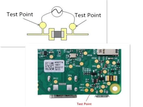
Testpoints are essential components in PCB design that facilitate testing, debugging, and troubleshooting of electronic circuits. These strategically placed points on a printed circuit board allow engineers and technicians to easily access and measure critical signals, voltages, and other parameters without the need for probing or soldering. By incorporating testpoints into the PCB layout, designers can significantly improve the manufacturability, reliability, and maintainability of their electronic products.
In this comprehensive article, we will explore the importance of adding testpoints to PCBs, discuss various types of testpoints, and provide guidelines for their effective placement and usage. We will also delve into the benefits of utilizing testpoints in different stages of the product development cycle and share best practices for optimizing their implementation in PCB designs.
Understanding the Importance of Testpoints in PCB Design
Testpoints serve several crucial functions in PCB design and manufacturing processes. They enable engineers to:
-
Verify functionality: Testpoints allow engineers to confirm that the PCB is functioning as intended by providing access points for measuring signals, voltages, and other parameters. This helps in identifying and resolving issues early in the development process.
-
Facilitate debugging: When a PCB malfunctions or exhibits unexpected behavior, testpoints provide a means to isolate and diagnose the problem. By probing specific testpoints, engineers can pinpoint the source of the issue and take corrective actions.
-
Streamline manufacturing: Testpoints play a vital role in the manufacturing process by enabling automated testing and quality control. Automated test equipment (ATE) can quickly and efficiently test PCBs by accessing the designated testpoints, ensuring consistent quality and reducing human error.
-
Simplify maintenance and repairs: In the event of a device failure or required maintenance, testpoints allow technicians to easily troubleshoot and repair the PCB without the need for extensive disassembly or specialized tools.
Types of Testpoints Used in PCB Design
There are several types of testpoints commonly used in PCB design, each with its own characteristics and applications. The most common types include:
-
Through-hole testpoints: These testpoints are drilled through the PCB and have a conductive pad on both sides. They provide a robust and reliable connection for probing and are suitable for manual testing and debugging.
-
Surface mount testpoints: Surface mount testpoints are placed on the surface of the PCB and do not require drilling. They are smaller in size compared to through-hole testpoints and are ideal for automated testing and high-density PCB designs.
-
Edge connector testpoints: These testpoints are located along the edge of the PCB and are accessible through the edge connector. They are commonly used for in-circuit testing and provide easy access to critical signals without the need for probing the PCB surface.
-
Bed-of-nails testpoints: Bed-of-nails testpoints are arranged in a grid pattern and are designed to mate with a specialized test fixture. This type of testpoint is often used for high-volume manufacturing and enables rapid testing of multiple PCBs simultaneously.
| Testpoint Type | Characteristics | Applications |
|---|---|---|
| Through-hole | – Drilled through PCB – Conductive pad on both sides – Robust and reliable |
– Manual testing and debugging |
| Surface mount | – Placed on PCB surface – Smaller in size – No drilling required |
– Automated testing – High-density PCB designs |
| Edge connector | – Located along PCB edge – Accessible through edge connector |
– In-circuit testing – Easy access to critical signals |
| Bed-of-nails | – Arranged in grid pattern – Mates with specialized test fixture |
– High-volume manufacturing – Rapid testing of multiple PCBs |

Guidelines for Effective Testpoint Placement
Proper placement of testpoints is crucial for their effectiveness and usability. When deciding where to place testpoints on a PCB, consider the following guidelines:
-
Accessibility: Testpoints should be easily accessible for probing or connecting test equipment. Ensure that they are not obstructed by components, connectors, or other features on the PCB.
-
Signal integrity: Place testpoints close to the source of the signal being measured to minimize the impact of signal degradation and interference. Avoid placing testpoints in areas with high-speed signals or sensitive analog circuits.
-
Electrical considerations: Testpoints should not introduce excessive capacitance or loading on the circuit being tested. Use appropriate testpoint sizes and materials to minimize their impact on the electrical characteristics of the PCB.
-
Manufacturing compatibility: Consider the manufacturing process when placing testpoints. Ensure that they do not interfere with the placement of other components or violate design rules related to minimum spacing and clearance.
-
Labeling and documentation: Clearly label testpoints on the PCB silkscreen and provide comprehensive documentation, including testpoint locations, signal names, and expected values. This facilitates efficient testing and troubleshooting.
Best Practices for Optimizing Testpoint Usage
To maximize the benefits of testpoints in PCB design, consider the following best practices:
-
Standardize testpoint placement: Develop a consistent approach to testpoint placement across different PCB designs. This promotes familiarity among engineers and technicians and reduces the learning curve when working with new designs.
-
Use dedicated test pads: Incorporate dedicated test pads or vias for critical signals or power rails. These pads provide a reliable and consistent point for probing and can be sized appropriately for the intended test equipment.
-
Implement testpoint numbering: Assign unique identifiers or numbers to each testpoint on the PCB. This helps in referencing specific testpoints in documentation, test procedures, and communication among team members.
-
Leverage automated testing: Utilize automated test equipment and software to streamline the testing process. Automated tests can quickly verify the functionality of the PCB by accessing the designated testpoints, reducing testing time and improving overall efficiency.
-
Collaborate with manufacturing partners: Engage with your manufacturing partners early in the design process to discuss testpoint requirements and compatibility with their testing equipment and processes. This collaboration ensures smooth integration of testpoints into the manufacturing workflow.

Benefits of Testpoints in Different Stages of Product Development
Incorporating testpoints into PCB designs offers benefits throughout the product development lifecycle, from prototyping to production and field maintenance.
Prototyping and Validation
During the prototyping and validation stage, testpoints enable engineers to:
– Verify the functionality of individual circuits and subsystems
– Debug and troubleshoot issues encountered during initial testing
– Validate the performance of the PCB against design specifications
– Optimize the design based on real-world measurements and feedback
Manufacturing and Quality Control
In the manufacturing and quality control phase, testpoints play a crucial role in:
– Automated testing of PCBs using dedicated test equipment
– Ensuring consistent quality across production batches
– Identifying and isolating faulty components or assembly issues
– Reducing manufacturing costs by catching defects early in the process
Field Maintenance and Repairs
Testpoints continue to provide value even after the product is deployed in the field. They enable:
– On-site troubleshooting and diagnosis of issues
– Efficient repairs and component replacements
– Simplified maintenance procedures for service technicians
– Reduced downtime and improved customer satisfaction

Frequently Asked Questions (FAQ)
-
What is the purpose of adding testpoints to a PCB?
Testpoints are added to PCBs to facilitate testing, debugging, and troubleshooting of electronic circuits. They provide access points for measuring critical signals, voltages, and other parameters without the need for probing or soldering. -
How do testpoints improve the manufacturing process?
Testpoints enable automated testing and quality control in the manufacturing process. Automated test equipment can quickly and efficiently test PCBs by accessing the designated testpoints, ensuring consistent quality and reducing human error. -
What are the different types of testpoints used in PCB design?
The most common types of testpoints used in PCB design include through-hole testpoints, surface mount testpoints, edge connector testpoints, and bed-of-nails testpoints. Each type has its own characteristics and applications. -
What factors should be considered when placing testpoints on a PCB?
When placing testpoints on a PCB, consider factors such as accessibility, signal integrity, electrical considerations, manufacturing compatibility, and labeling/documentation. Proper placement ensures the effectiveness and usability of the testpoints. -
How can testpoints benefit the product development lifecycle?
Testpoints offer benefits throughout the product development lifecycle, including prototyping and validation, manufacturing and quality control, and field maintenance and repairs. They enable efficient testing, debugging, troubleshooting, and maintenance of electronic products.
Conclusion
Adding testpoints to PCBs is a crucial aspect of electronic design that contributes to the overall quality, reliability, and maintainability of the final product. By providing accessible points for testing, debugging, and troubleshooting, testpoints streamline the development process, improve manufacturing efficiency, and simplify field maintenance.
When incorporating testpoints into PCB designs, it is essential to consider factors such as accessibility, signal integrity, manufacturing compatibility, and proper labeling. By following best practices and leveraging automated testing techniques, engineers can optimize the usage of testpoints and realize their full potential in various stages of the product development lifecycle.
As electronic products continue to advance in complexity and functionality, the importance of testpoints in PCB design will only continue to grow. By embracing the benefits of testpoints and implementing them effectively, engineers can develop more robust, reliable, and easily maintainable electronic products that meet the demands of today’s competitive market.

No responses yet