Introduction to Multilayer PCB
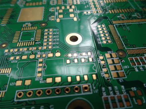
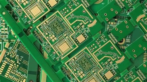
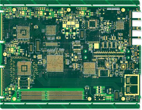
Printed Circuit Boards (PCBs) are essential components in modern electronic devices, providing a platform for interconnecting electronic components. As technology advances and devices become more complex, the demand for high-density and compact PCBs increases. This is where multilayer PCBs come into play. Multilayer PCBs consist of multiple layers of conductive material, separated by insulating layers, allowing for a higher component density and more complex circuit designs.
What is a Multilayer PCB?
A multilayer PCB is a printed circuit board that consists of three or more conductive layers, separated by insulating layers. The conductive layers are typically made of copper, while the insulating layers are made of materials such as FR-4, a glass-reinforced epoxy laminate. The layers are bonded together using heat and pressure, forming a single, compact board.
Advantages of Multilayer PCBs
Multilayer PCBs offer several advantages over single or double-layer PCBs:
- Higher component density: With multiple layers, more components can be accommodated in a smaller space, resulting in more compact devices.
- Improved signal integrity: The use of dedicated power and ground planes in multilayer PCBs reduces electromagnetic interference (EMI) and improves signal quality.
- Increased reliability: The compact design and reduced EMI of multilayer PCBs lead to improved reliability and longer product life.
- Reduced costs: Although the initial cost of multilayer PCBs may be higher, the increased functionality and reduced size can lead to overall cost savings in the long run.
Determining Your Multilayer PCB Requirements
When deciding on the specifications for your multilayer PCB, there are several factors to consider:
Number of Layers
The number of layers in your multilayer PCB will depend on the complexity of your circuit design and the space constraints of your device. A higher number of layers allows for more complex routing and higher component density but also increases the cost and manufacturing complexity.
| Number of Layers | Complexity | Cost | Manufacturing Difficulty |
|---|---|---|---|
| 4 | Low | Low | Low |
| 6-8 | Medium | Medium | Medium |
| 10+ | High | High | High |
Layer Stack-up
The layer stack-up refers to the arrangement of conductive and insulating layers in your multilayer PCB. A typical stack-up might include:
- Top layer: Components and signal routing
- Ground plane
- Signal layers
- Power plane
- Signal layers
- Bottom layer: Components and signal routing
The exact stack-up will depend on your circuit requirements and the number of layers in your PCB.
Material Selection
The choice of materials for your multilayer PCB will impact its performance, reliability, and cost. The most common materials used are:
- FR-4: A glass-reinforced epoxy laminate, offering good mechanical and electrical properties at a reasonable cost.
- High-Tg FR-4: A variant of FR-4 with improved thermal stability, suitable for high-temperature applications.
- Polyimide: A high-performance material with excellent thermal and mechanical properties, but at a higher cost.
Trace Width and Spacing
The width and spacing of the traces on your multilayer PCB will depend on the current carrying requirements and the manufacturing capabilities of your PCB supplier. Smaller trace widths allow for higher component density but also increase the manufacturing complexity and cost.
| Trace Width (mm) | Current Capacity (A) | Manufacturing Difficulty |
|---|---|---|
| 0.2 | 0.5 | High |
| 0.3 | 1.0 | Medium |
| 0.5 | 2.0 | Low |
Via Types and Sizes
Vias are used to interconnect the layers in your multilayer PCB. The type and size of vias will depend on your circuit requirements and the manufacturing capabilities of your PCB supplier. Common via types include:
- Through-hole vias: Drilled holes that interconnect all layers.
- Blind vias: Drilled holes that interconnect only some of the layers, starting from an outer layer.
- Buried vias: Drilled holes that interconnect only inner layers, not reaching the outer layers.
The size of the vias will depend on the current carrying requirements and the manufacturing capabilities of your PCB supplier.

Designing Your Multilayer PCB
Once you have determined your multilayer PCB requirements, the next step is to design your PCB. The design process typically involves the following steps:
- Schematic capture: Creating a schematic diagram of your circuit, specifying the components and their interconnections.
- Component placement: Arranging the components on the PCB layout, taking into account factors such as signal integrity, thermal management, and manufacturability.
- Routing: Interconnecting the components using traces on the various layers of the PCB, following the design rules specified by your PCB supplier.
- Design rule check (DRC): Verifying that your PCB layout meets the design rules, such as minimum trace widths and spacings, via sizes, and clearances.
- Gerber file generation: Creating the final manufacturing files, including the Gerber files for each layer and the drill files for the vias.
PCB Design Software
There are several PCB design software packages available, ranging from free and open-source to commercial and high-end. Some popular options include:
- KiCad: A free and open-source PCB design package, offering schematic capture, PCB layout, and 3D viewing capabilities.
- Eagle: A commercial PCB design package, widely used by hobbyists and small businesses, offering schematic capture, PCB layout, and autorouting capabilities.
- Altium Designer: A high-end commercial PCB design package, offering advanced features such as Multi-Board Design, signal integrity analysis, and 3D modeling.

Manufacturing Your Multilayer PCB
Once your multilayer PCB design is complete, the next step is to manufacture the board. The manufacturing process typically involves the following steps:
- PCB fabrication: The PCB manufacturer creates the individual layers of your PCB using a photolithographic process, etching away the unwanted copper to create the traces and pads.
- Lamination: The individual layers are aligned and bonded together using heat and pressure, forming the complete multilayer PCB.
- Drilling: Holes are drilled through the PCB for through-hole components and vias.
- Plating: The drilled holes are plated with copper to create electrical connections between the layers.
- Solder mask application: A protective solder mask is applied to the outer layers of the PCB, exposing only the pads and vias that require soldering.
- Silkscreen printing: Text and symbols are printed on the outer layers of the PCB for component identification and assembly instructions.
- Surface finish application: A surface finish, such as HASL (Hot Air Solder Leveling) or ENIG (Electroless Nickel Immersion Gold), is applied to the exposed copper to prevent oxidation and improve solderability.
- Electrical testing: The completed PCB is electrically tested to ensure that all connections are correct and there are no short circuits or open connections.
Choosing a PCB Manufacturer
When choosing a PCB manufacturer, there are several factors to consider:
- Manufacturing capabilities: Ensure that the manufacturer can handle the complexity of your multilayer PCB, including the number of layers, minimum trace widths and spacings, and via types and sizes.
- Quality control: Look for a manufacturer with a robust quality control process, including automated optical inspection (AOI) and electrical testing.
- Lead times: Consider the manufacturer’s lead times, especially if you have tight deadlines for your project.
- Cost: Obtain quotes from multiple manufacturers to ensure you are getting a competitive price for your multilayer PCB.

Assembling Your Multilayer PCB
After your multilayer PCB has been manufactured, the final step is to assemble the components onto the board. This process typically involves the following steps:
- Solder paste application: Solder paste is applied to the pads on the PCB using a stencil or syringe.
- Component placement: The components are placed onto the PCB, either manually or using automated pick-and-place equipment.
- Reflow soldering: The PCB is heated in a reflow oven, melting the solder paste and creating electrical connections between the components and the PCB.
- Inspection: The assembled PCB is visually inspected for any defects, such as misaligned components or solder bridges.
- Functional testing: The assembled PCB is functionally tested to ensure that it performs as intended.
PCB Assembly Services
If you do not have the equipment or expertise to assemble your multilayer PCB in-house, there are several PCB assembly services available. These services typically offer turnkey solutions, including component sourcing, PCB assembly, and functional testing.
When choosing a PCB assembly service, consider factors such as:
- Capabilities: Ensure that the service can handle the complexity of your multilayer PCB and the types of components you are using.
- Quality control: Look for a service with a robust quality control process, including automated optical inspection (AOI) and functional testing.
- Lead times: Consider the service’s lead times, especially if you have tight deadlines for your project.
- Cost: Obtain quotes from multiple services to ensure you are getting a competitive price for your PCB assembly.
Frequently Asked Questions (FAQ)
- What is the minimum number of layers required for a multilayer PCB?
-
A multilayer PCB requires at least three conductive layers, separated by insulating layers.
-
What are the advantages of using a multilayer PCB over a single or double-layer PCB?
-
Multilayer PCBs offer higher component density, improved signal integrity, increased reliability, and potential cost savings compared to single or double-layer PCBs.
-
What factors should I consider when determining the number of layers for my multilayer PCB?
-
The number of layers in your multilayer PCB will depend on the complexity of your circuit design, the space constraints of your device, and your budget. A higher number of layers allows for more complex routing and higher component density but also increases the cost and manufacturing complexity.
-
What are the most common materials used for multilayer PCBs?
-
The most common materials used for multilayer PCBs are FR-4 (a glass-reinforced epoxy laminate), high-Tg FR-4 (a variant of FR-4 with improved thermal stability), and polyimide (a high-performance material with excellent thermal and mechanical properties).
-
What should I look for when choosing a PCB manufacturer for my multilayer PCB?
- When choosing a PCB manufacturer, consider factors such as their manufacturing capabilities (including the number of layers, minimum trace widths and spacings, and via types and sizes they can handle), quality control processes, lead times, and cost. Obtain quotes from multiple manufacturers to ensure you are getting a competitive price for your multilayer PCB.
Conclusion
Multilayer PCBs are essential components in modern electronic devices, offering high component density, improved signal integrity, and increased reliability. When determining your multilayer PCB requirements, consider factors such as the number of layers, layer stack-up, material selection, trace width and spacing, and via types and sizes.
Designing your multilayer PCB involves schematic capture, component placement, routing, design rule checking, and Gerber file generation. There are several PCB design software packages available, ranging from free and open-source to commercial and high-end.
Manufacturing your multilayer PCB involves PCB fabrication, lamination, drilling, plating, solder mask application, silkscreen printing, surface finish application, and electrical testing. When choosing a PCB manufacturer, consider their manufacturing capabilities, quality control processes, lead times, and cost.
Assembling your multilayer PCB involves solder paste application, component placement, reflow soldering, inspection, and functional testing. If you do not have the equipment or expertise to assemble your multilayer PCB in-house, there are several PCB assembly services available, offering turnkey solutions.
By understanding the factors involved in determining your multilayer PCB requirements, designing your PCB, and manufacturing and assembling your board, you can ensure that your electronic device meets its performance, reliability, and cost targets.

No responses yet