Introduction to PCB Prototyping
PCB prototyping is an essential process in the development of electronic devices. It involves creating a physical model of a printed circuit board (PCB) to test and validate its functionality before mass production. PCB prototyping allows designers and engineers to identify and fix any issues with the design, ensuring that the final product meets the required specifications and performs as expected.
In this article, we will discuss 8 key matters you need to pay attention to when it comes to PCB prototyping. These include:
- Design Software and Tools
- PCB Material Selection
- Component Placement and Routing
- Design for Manufacturability (DFM)
- Prototype Fabrication Methods
- Testing and Validation
- Documentation and Version Control
- Choosing the Right PCB Prototyping Partner
By understanding and addressing these matters, you can streamline your PCB prototyping process, reduce costs, and improve the overall quality of your electronic devices.
1. Design Software and Tools
Choosing the right design software and tools is crucial for successful PCB prototyping. There are various options available in the market, each with its own strengths and weaknesses. Some of the popular PCB design software include:
- Altium Designer
- Cadence OrCAD
- KiCad
- Eagle CAD
- Mentor Graphics PADS
When selecting a design software, consider factors such as ease of use, compatibility with your existing tools and workflows, and the availability of libraries and components. It’s also essential to ensure that the software supports the necessary file formats for fabrication and assembly.
In addition to design software, you may also need other tools such as:
- Schematic capture tools for creating circuit diagrams
- Simulation tools for analyzing and optimizing the circuit’s performance
- 3D modeling tools for visualizing the PCB and its components
- Gerber viewers for checking the accuracy of the generated files

2. PCB Material Selection
The choice of PCB material can significantly impact the performance, reliability, and cost of your prototype. There are several factors to consider when selecting the appropriate PCB material, including:
- Dielectric constant (Dk) and dissipation factor (Df)
- Thermal conductivity
- Mechanical strength and flexibility
- Cost and availability
Some of the common PCB materials include:
| Material | Dielectric Constant (Dk) | Dissipation Factor (Df) | Thermal Conductivity (W/mK) | Applications |
|---|---|---|---|---|
| FR-4 | 4.2-4.6 | 0.02-0.03 | 0.3-0.4 | General-purpose, low-cost |
| Rogers 4350B | 3.48 | 0.0037 | 0.62 | High-frequency, RF/microwave |
| Polyimide | 3.4-3.5 | 0.002-0.003 | 0.2-0.3 | Flexible, high-temperature |
| Alumina | 9.8-10.2 | 0.0001-0.0005 | 25-35 | High-frequency, high-power |
Choose the PCB material that best suits your application’s requirements, considering factors such as the operating frequency, environmental conditions, and budget constraints.

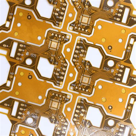
3. Component Placement and Routing
Proper component placement and routing are essential for ensuring the optimal performance and manufacturability of your PCB Prototype. When placing components on the board, consider the following guidelines:
- Group related components together to minimize the length of traces and improve signal integrity
- Place components on both sides of the board to maximize space utilization
- Ensure adequate clearance between components to allow for easy assembly and rework
- Orient components in a consistent direction to simplify the assembly process
Once the components are placed, you need to route the traces that connect them. Some best practices for PCB routing include:
- Use the shortest possible traces to minimize signal loss and interference
- Avoid sharp angles and use smooth curves to reduce signal reflections
- Maintain consistent trace width and spacing to ensure uniform impedance
- Use ground planes and power planes to provide a low-impedance return path and reduce noise
- Avoid routing traces under components or vias to prevent signal integrity issues
By following these guidelines, you can create a well-organized and efficient PCB layout that minimizes the risk of manufacturing defects and ensures optimal performance.

4. Design for Manufacturability (DFM)
Design for Manufacturability (DFM) is a crucial aspect of PCB prototyping that aims to optimize the design for efficient and cost-effective manufacturing. By incorporating DFM principles into your design process, you can reduce the risk of manufacturing defects, improve yield, and lower production costs.
Some key DFM considerations include:
- Minimum trace width and spacing: Ensure that your design adheres to the fabrication house’s minimum requirements for trace width and spacing to avoid manufacturing issues.
- Drill sizes and pad sizes: Use standard drill sizes and pad sizes to minimize the cost and lead time for fabrication.
- Solder mask and silkscreen: Provide adequate clearance between components and solder mask openings to ensure proper solder joint formation. Use clear and legible silkscreen markings to aid in assembly and debugging.
- Panelization: Consider panelizing your design to maximize the number of boards per panel and reduce the cost per board.
- Testability: Incorporate test points and other features that facilitate testing and debugging of the assembled board.
By working closely with your PCB fabrication and assembly partners and following their DFM guidelines, you can ensure that your PCB prototype is optimized for manufacturability and can be easily scaled up for mass production.
5. Prototype Fabrication Methods
There are several methods for fabricating PCB prototypes, each with its own advantages and limitations. The choice of fabrication method depends on factors such as the complexity of the design, the required turnaround time, and the budget.
Some common PCB prototype fabrication methods include:
- Quick-turn PCB services: These services offer fast turnaround times (typically 1-5 days) for low-volume prototypes. They use standard materials and processes to keep costs low and lead times short.
- In-house PCB milling: This method involves using a CNC milling machine to route the traces and drill the holes on a blank PCB substrate. It is suitable for simple designs and quick iterations but may not be as precise or reliable as other methods.
- 3D printing: 3D printing can be used to create PCB prototypes by depositing conductive and insulating materials layer by layer. This method is suitable for complex geometries and rapid prototyping but may not be as durable or precise as traditional methods.
- Traditional PCB fabrication: This involves the standard process of etching, drilling, and plating the PCB using photolithography and chemical processes. It offers the highest quality and precision but may have longer lead times and higher costs for low volumes.
Choose the fabrication method that best suits your needs based on the complexity of your design, the required turnaround time, and your budget constraints.
6. Testing and Validation
Testing and validation are critical steps in the PCB prototyping process to ensure that the board functions as intended and meets the required specifications. There are various types of tests that can be performed at different stages of the prototyping process, including:
- Design rule checking (DRC): This involves checking the PCB layout against a set of design rules to ensure that it meets the fabrication house’s requirements for minimum trace width, spacing, and other parameters.
- Electrical rule checking (ERC): This checks the schematic for any electrical issues such as short circuits, open circuits, or incorrect connections.
- Simulation: Running simulations on the circuit can help identify potential issues with signal integrity, power distribution, and other aspects of the design before fabricating the prototype.
- In-circuit testing (ICT): This involves testing the assembled PCB using a bed-of-nails fixture to verify that all components are correctly placed and soldered and that the board functions as expected.
- Functional testing: This involves testing the assembled PCB in its intended application to ensure that it meets the required performance and reliability specifications.
By thoroughly testing and validating your PCB prototype, you can identify and fix any issues early in the development process, reducing the risk of costly rework or redesign later on.
7. Documentation and Version Control
Proper documentation and version control are essential for ensuring the traceability and reproducibility of your PCB prototype. Some key aspects of documentation and version control include:
- Schematic and layout files: Maintain a clear and organized set of schematic and layout files that accurately reflect the current version of the design. Use a consistent naming convention and directory structure to ensure easy access and retrieval.
- Bill of Materials (BOM): Create a detailed BOM that lists all the components used in the design, including their part numbers, quantities, and suppliers. Keep the BOM updated as the design evolves to ensure accurate procurement and assembly.
- Fabrication and assembly files: Generate and maintain a complete set of fabrication and assembly files, including Gerber files, drill files, and pick-and-place files. Ensure that these files are properly formatted and checked for accuracy before sending them to the fabrication and assembly houses.
- Revision history: Keep track of all changes made to the design, including the reason for the change, the date, and the person responsible. Use a version control system such as Git or SVN to manage the revision history and facilitate collaboration among team members.
By maintaining accurate and up-to-date documentation and version control, you can ensure that your PCB prototype can be easily reproduced and scaled up for mass production.
8. Choosing the Right PCB Prototyping Partner
Choosing the right PCB prototyping partner is crucial for ensuring the success of your project. A good prototyping partner should have the expertise, capabilities, and resources to deliver high-quality prototypes on time and within budget.
Some factors to consider when choosing a PCB prototyping partner include:
- Experience and expertise: Look for a partner with a proven track record of successfully delivering PCB prototypes for a wide range of applications and industries.
- Technology and capabilities: Ensure that the partner has the necessary equipment and processes to fabricate and assemble your prototype to the required specifications and tolerances.
- Quality and reliability: Choose a partner that has a robust quality management system and follows industry-standard practices for ensuring the quality and reliability of their products.
- Communication and support: Look for a partner that provides clear and responsive communication throughout the prototyping process and offers technical support and guidance as needed.
- Cost and lead time: Consider the partner’s pricing and lead times for different prototyping options and choose the one that best fits your budget and timeline constraints.
By carefully evaluating and selecting the right PCB prototyping partner, you can ensure that your project stays on track and delivers the desired results.
Frequently Asked Questions (FAQ)
- What is the typical turnaround time for PCB prototyping?
-
The turnaround time for PCB prototyping varies depending on the complexity of the design and the fabrication method used. Quick-turn PCB services can deliver prototypes in as little as 1-5 days, while traditional PCB fabrication may take 1-2 weeks or longer.
-
How much does PCB prototyping cost?
-
The cost of PCB prototyping depends on factors such as the size and complexity of the board, the number of layers, the quantity ordered, and the fabrication method used. Quick-turn PCB services typically charge a premium for fast turnaround times, while traditional PCB fabrication may offer lower prices for higher volumes.
-
What is the minimum order quantity (MOQ) for PCB prototypes?
-
The MOQ for PCB prototypes varies depending on the fabrication method and the service provider. Some quick-turn PCB services offer prototypes with no minimum order quantity, while others may require a minimum of 5-10 pieces. Traditional PCB fabrication typically requires a minimum order of 50-100 pieces or more.
-
What file formats are required for PCB prototyping?
-
The file formats required for PCB prototyping include Gerber files (RS-274X) for the PCB layout, drill files (Excellon) for the hole locations and sizes, and pick-and-place files (CSV or TXT) for the component placement. Some fabrication houses may also require additional files such as the bill of materials (BOM) and the assembly drawings.
-
How can I ensure the quality and reliability of my PCB prototype?
- To ensure the quality and reliability of your PCB prototype, follow best practices for design, fabrication, and assembly, such as adhering to the fabrication house’s design rules, using high-quality components and materials, and thoroughly testing and validating the assembled board. Choosing a reputable and experienced PCB prototyping partner can also help ensure the quality and reliability of your prototype.
Conclusion
PCB prototyping is a critical step in the development of electronic devices, allowing designers and engineers to test and validate their designs before committing to mass production. By paying attention to the 8 key matters discussed in this article, including design software and tools, PCB material selection, component placement and routing, design for manufacturability, prototype fabrication methods, testing and validation, documentation and version control, and choosing the right PCB prototyping partner, you can streamline your prototyping process, reduce costs, and improve the overall quality and reliability of your electronic devices.
No responses yet